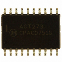
MC74ACT273DWG ON Semiconductor, MC74ACT273DWG Datasheet - Page 3

MC74ACT273DWG
Manufacturer Part Number
MC74ACT273DWG
Description
IC FLIP FLOP OCTAL D 20-SOIC
Manufacturer
ON Semiconductor
Series
74ACTr
Type
D-Type Busr
Datasheet
1.MC74AC273DTR2G.pdf
(8 pages)
Specifications of MC74ACT273DWG
Function
Master Reset
Output Type
Non-Inverted
Number Of Elements
1
Number Of Bits Per Element
8
Frequency - Clock
200MHz
Delay Time - Propagation
6.5ns
Trigger Type
Positive Edge
Current - Output High, Low
24mA, 24mA
Voltage - Supply
4.5 V ~ 5.5 V
Operating Temperature
-40°C ~ 85°C
Mounting Type
Surface Mount
Package / Case
20-SOIC (7.5mm Width)
Number Of Circuits
8
Logic Family
74AC
Logic Type
D-Type Flip-Flop
Polarity
Non-Inverting
Input Type
Single-Ended
Propagation Delay Time
11 ns
High Level Output Current
- 24 mA
Supply Voltage (max)
5.5 V
Maximum Operating Temperature
+ 85 C
Mounting Style
SMD/SMT
Minimum Operating Temperature
- 40 C
Supply Voltage (min)
4.5 V
Lead Free Status / RoHS Status
Lead free / RoHS Compliant
Other names
MC74ACT273DWG
MC74ACT273DWGOS
MC74ACT273DWGOS
Available stocks
Company
Part Number
Manufacturer
Quantity
Price
Company:
Part Number:
MC74ACT273DWG
Manufacturer:
ON Semiconductor
Quantity:
16
*All outputs loaded; thresholds on input associated with output under test.
†Maximum test duration 2.0 ms, one output loaded at a time.
NOTE:
*Voltage Range 3.3 V is 3.3 V ±0.3 V. Voltage Range 5.0 V is 5.0 V ±0.5 V.
*Voltage Range 3.3 V is 3.3 V ±0.3 V. Voltage Range 5.0 V is 5.0 V ±0.5 V.
DC CHARACTERISTICS
AC CHARACTERISTICS
AC OPERATING REQUIREMENTS
Symbol
Symbol
Symbol
I
I
V
f
t
t
t
V
V
OHD
V
OLD
I
t
max
PLH
PHL
PHL
I
CC
t
t
rec
t
t
OH
OL
IN
w
w
IH
s
h
IL
Note: I
Minimum High Level Input Voltage
Maximum Low Level Input Voltage
Minimum High Level Output Voltage
Maximum Low Level Output Voltage
Maximum Input Leakage Current
†Minimum Dynamic Output Current
Maximum Quiescent Supply Current
Maximum Clock
Frequency
Propagation Delay
Clock to Output
Propagation Delay
Clock to Output
Propagation Delay
MR to Output
Setup Time, HIGH or LOW
Data to CP
Hold Time, HIGH or LOW
Data to CP
Clock Pulse Width
HIGH or LOW
MR Pulse Width
HIGH or LOW
Recovery Time
MR to CP
IN
and I
CC
Parameter
Parameter
@ 3.0 V are guaranteed to be less than or equal to the respective limit @ 5.5 V V
Parameter
(For Figures and Waveforms − See Section 3 of the ON Semiconductor FACT Data Book, DL138/D)
V
MC74AC273, MC74ACT273
(V)
3.3
5.0
3.3
5.0
3.3
5.0
3.3
5.0
CC
V
(V)
3.3
5.0
3.3
5.0
3.3
5.0
3.3
5.0
3.3
5.0
CC
*
*
V
(V)
3.0
4.5
5.5
3.0
4.5
5.5
3.0
4.5
5.5
3.0
4.5
5.5
3.0
4.5
5.5
3.0
4.5
5.5
5.5
5.5
5.5
5.5
CC
Min
140
http://onsemi.com
T
4.0
3.0
4.0
3.0
4.0
3.0
T
90
A
A
−2.0
−1.0
= +25°C C
= +25°C C
Typ
3.5
2.5
3.5
2.5
2.0
1.5
1.5
1.0
0.002
0.001
0.001
2.25
2.75
2.25
2.75
2.99
4.49
5.49
Typ
1.5
1.5
T
−
−
−
−
−
−
−
−
−
−
74AC
74AC
A
Typ
125
175
7.0
5.5
7.0
5.0
7.0
5.0
3
74AC
= +25°C
L
L
= 50 pF
= 50 pF
5.5
4.0
1.0
5.5
4.0
5.5
4.0
3.5
2.0
3.15
3.85
1.35
1.65
2.56
3.86
4.86
0.36
0.36
0.36
±0.1
2.1
0.9
2.9
4.4
5.4
0.1
0.1
0.1
8.0
0
−
−
Max
12.5
13.0
10.0
13.0
10.0
9.0
Guaranteed Limits
−
−
Guaranteed Minimum
T
T
A
A
T
= −40°C to +85°C
A
= −40°C to +85°C C
= −40°C to +85°C C
74AC
3.15
3.85
1.35
1.65
2.46
3.76
4.76
0.44
0.44
0.44
±1.0
Min
125
−75
3.0
2.5
3.5
2.5
3.5
2.5
2.1
0.9
2.9
4.4
5.4
0.1
0.1
0.1
75
75
80
74AC
6.0
4.5
1.0
6.0
4.5
6.0
4.5
4.5
3.0
74AC
0
L
CC
Unit
mA
Max
14.0
10.0
14.5
14.0
10.5
mA
mA
L
11.0
= 50 pF
V
V
V
V
V
V
−
−
.
= 50 pF
V
or V
V
or V
I
*V
I
I
*V
I
V
V
V
V
OUT
OH
OUT
OL
OUT
OUT
I
OLD
OHD
IN
IN
IN
= V
= V
CC
CC
Conditions
= V
= V
= −50 mA
= 50 mA
Unit
Unit
Mhz
= 1.65 V Max
= 0.1 V
= 0.1 V
CC
= 3.85 V Min
ns
ns
ns
ns
ns
ns
ns
ns
− 0.1 V
− 0.1 V
CC
IL
IL
, GND
−12 mA
−24 mA
−24 mA
12 mA
24 mA
24 mA
or V
or V
or GND
Figure
Figure
IH
IH
3−3
3−6
3−6
3−6
3−9
3−9
3−6
3−6
3−9
No.
No.


