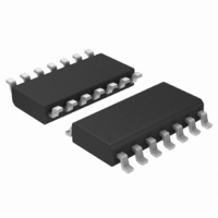
MC74ACT74DG ON Semiconductor, MC74ACT74DG Datasheet - Page 2

MC74ACT74DG
Manufacturer Part Number
MC74ACT74DG
Description
IC FLIP FLOP DUAL TYPE D 14-SOIC
Manufacturer
ON Semiconductor
Series
74ACTr
Type
D-Typer
Datasheet
1.MC74AC74DR2G.pdf
(12 pages)
Specifications of MC74ACT74DG
Function
Set(Preset) and Reset
Output Type
Differential
Number Of Elements
2
Number Of Bits Per Element
1
Frequency - Clock
210MHz
Delay Time - Propagation
5.5ns
Trigger Type
Positive Edge
Current - Output High, Low
24mA, 24mA
Voltage - Supply
4.5 V ~ 5.5 V
Operating Temperature
-40°C ~ 85°C
Mounting Type
Surface Mount
Package / Case
14-SOIC (3.9mm Width), 14-SOL
Number Of Circuits
2
Logic Family
74ACT
Logic Type
D-Type Edge Triggered Flip-Flop
Polarity
Inverting/Non-Inverting
Input Type
Single-Ended
Propagation Delay Time
11 ns
High Level Output Current
- 24 mA
Low Level Output Current
24 mA
Supply Voltage (max)
5.5 V
Maximum Operating Temperature
+ 85 C
Mounting Style
SMD/SMT
Minimum Operating Temperature
- 40 C
Supply Voltage (min)
4.5 V
Rohs Compliant
YES
Flip-flop Type
D
Propagation Delay
6ns
Frequency
160MHz
Output Current
24mA
Ic Output Type
Complementary
Supply Voltage Range
4.5V To 5.5V
Lead Free Status / RoHS Status
Lead free / RoHS Compliant
Other names
MC74ACT74DG
MC74ACT74DGOS
MC74ACT74DGOS
NOTE:
Stresses exceeding Maximum Ratings may damage the device. Maximum Ratings are stress ratings only. Functional operation above the
Recommended Operating Conditions is not implied. Extended exposure to stresses above the Recommended Operating Conditions may affect
device reliability.
TRUTH TABLE (Each Half)
MAXIMUM RATINGS
V
V
V
I
I
I
T
in
out
CC
stg
out
CC
in
S
H
H
H
H
L
L
D
Symbol
H = HIGH Voltage Level
L = LOW Voltage Level
X = Immaterial;
Q
0
CP
S
C
(Q
D
D
D
0
C
H
H
H
H
= LOW-to-HIGH Clock Transition
) = Previous Q(Q) before LOW-to-HIGH
L
L
D
Inputs
Transition of Clock
DC Supply Voltage (Referenced to GND)
DC Input Voltage (Referenced to GND)
DC Output Voltage (Referenced to GND)
DC Input Current, per Pin
DC Output Sink/Source Current, per Pin
DC V
Storage Temperature
CP
CC
X
X
X
L
or GND Current per Output Pin
D
H
X
X
X
X
NOTE:
L
This diagram is provided only for the understanding of
logic operations and should not be used to estimate
propagation delays.
Q
Q
H
H
H
L
L
0
Outputs
Parameter
Figure 3. Logic Diagram
http://onsemi.com
Q
Q
H
H
H
L
L
0
2
Figure 2. Logic Symbol
S
S
D1
D2
Q
D
D
Q
1
1
2
2
−0.5 to V
−0.5 to V
CP
CP
−0.5 to +7.0
−65 to +150
1
2
Value
±20
±50
±50
Q
Q
CD
1
C
2
CC
CC
D1
2
+0.5
+0.5
Unit
mA
mA
mA
Q
Q
°C
V
V
V


