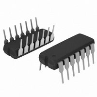
MC14011BCPG ON Semiconductor, MC14011BCPG Datasheet - Page 2

MC14011BCPG
Manufacturer Part Number
MC14011BCPG
Description
IC GATE NAND QUAD 2INPUT 14DIP
Manufacturer
ON Semiconductor
Series
4000Br
Specifications of MC14011BCPG
Logic Type
NAND Gate
Number Of Inputs
2
Number Of Circuits
4
Current - Output High, Low
3.4mA, 3.4mA
Voltage - Supply
3 V ~ 18 V
Operating Temperature
-55°C ~ 125°C
Mounting Type
Through Hole
Package / Case
14-DIP (0.300", 7.62mm)
Logic Family
4000
Logical Function
NAND
Number Of Elements
4
High Level Output Current
-4.2mA
Low Level Output Current
4.2mA
Propagation Delay Time
80ns
Operating Supply Voltage (typ)
3.3/5/9/12/15V
Operating Temp Range
-55C to 125C
Package Type
PDIP
Number Of Outputs
1
Technology
CMOS
Mounting
Through Hole
Pin Count
14
Operating Temperature Classification
Military
Quiescent Current
1uA
Operating Supply Voltage (max)
18V
Operating Supply Voltage (min)
3V
Product
NAND
Supply Voltage (max)
18 V
Supply Voltage (min)
3 V
Maximum Operating Temperature
+ 125 C
Mounting Style
Through Hole
Minimum Operating Temperature
- 55 C
Circuit Type
Low-Power Schottky
Current, Supply
30 μA
Function Type
2-Inputs
Logic Function
NAND Gate
Temperature, Operating, Range
-55 to +125 °C
Voltage, Supply
3 to 18 VDC
Output Current
8.8mA
No. Of Inputs
2
Supply Voltage Range
3V To 18V
Logic Case Style
DIP
No. Of Pins
14
Operating Temperature Range
-55°C To +125°C
Filter Terminals
DIP
Rohs Compliant
Yes
Family Type
4000 CMOS
Lead Free Status / RoHS Status
Lead free / RoHS Compliant
Other names
MC14011BCPGOS
Available stocks
Company
Part Number
Manufacturer
Quantity
Price
Company:
Part Number:
MC14011BCPG
Manufacturer:
ON
Quantity:
2 145
Part Number:
MC14011BCPG
Manufacturer:
ON/安森美
Quantity:
20 000
Triple 3−Input NOR Gate
Quad 2−Input NOR Gate
Quad 2−Input NOR Gate
OUT
OUT
OUT
OUT
Quad 2−Input OR Gate
IN 2
IN 1
IN 1
IN 2
IN 1
IN 1
IN 2
IN 2
12
13
12
13
11
V
V
1
2
5
6
8
9
1
2
8
3
4
5
SS
SS
A
A
A
B
B
B
A
A
A
B
B
B
MC14001B
MC14025B
MC14001B
MC14071B
1
2
3
4
5
6
7
1
2
3
4
5
6
7
NOR
14
13
12
10
14
13
12
10
11
11
9
8
9
8
V
IN 2
IN 1
OUT
OUT
IN 2
IN 1
V
IN 2
IN 1
OUT
OUT
IN 2
IN 1
DD
DD
D
D
C
C
D
D
C
C
3
4
10
11
9
6
10
D
C
D
C
Quad 2−Input NAND Gate
Triple 3−Input AND Gate
OUT
OUT
OUT
IN 1
IN 2
IN 1
IN 2
IN 1
IN 2
IN 1
IN 2
IN 3
Triple 3−Input NAND Gate
Quad 2−Input NAND Gate
V
V
12
13
12
13
11
1
2
5
6
8
9
1
2
8
3
4
5
SS
SS
A
A
A
B
B
B
A
A
B
B
B
B
MC14011B
MC14073B
1
2
3
4
5
6
7
1
2
3
4
5
6
7
MC14023B
MC14011B
NAND
14
13
12
10
14
13
12
10
11
11
9
8
9
8
PIN ASSIGNMENTS
LOGIC DIAGRAMS
http://onsemi.com
V
IN 2
IN 1
OUT
OUT
IN 2
IN 1
V
IN 3
IN 2
IN 1
OUT
OUT
IN 3
DD
DD
D
D
C
C
C
C
C
A
D
C
C
A
3
4
10
11
9
6
10
2
Triple 3−Input NAND Gate
Quad 2−Input AND Gate
OUT
OUT
OUT
IN 1
IN 2
IN 1
IN 2
IN 3
IN 1
IN 2
IN 1
IN 2
Triple 3−Input AND Gate
12
13
12
13
V
V
11
Quad 2−Input OR Gate
1
2
5
6
8
9
1
2
8
3
4
5
SS
SS
A
A
B
B
B
B
A
A
A
B
B
B
MC14023B
MC14081B
1
2
3
4
5
6
7
1
2
3
4
5
6
7
MC14073B
MC14071B
OR
14
13
12
10
14
13
12
10
11
11
9
8
9
8
OUT
OUT
IN 2
V
IN 3
IN 2
IN 1
OUT
OUT
IN 3
V
IN 2
IN 1
IN 1
DD
DD
FOR ALL DEVICES
C
C
C
C
A
D
D
D
C
C
C
A
3
4
10
11
9
6
10
V
V
DD
SS
= PIN 14
= PIN 7
Triple 3−Input NOR Gate
Dual 4−Input AND Gate
OUT
OUT
IN 1
IN 2
IN 1
IN 2
IN 3
IN 1
IN 2
IN 3
IN 4
Quad 2−Input AND Gate
V
V
Dual 4−Input AND Gate
12
13
10
12
11
NC
NC = NO CONNECTION
SS
SS
1
2
5
6
8
9
2
3
4
5
9
A
A
B
B
B
B
A
A
A
A
A
MC14082B
MC14025B
1
2
3
4
5
6
7
1
2
3
4
5
6
7
MC14081B
MC14082B
AND
NC = 6, 8
14
13
12
10
14
13
12
10
11
11
9
8
9
8
V
IN 3
IN 2
IN 1
OUT
OUT
IN 3
V
OUT
IN 4
IN 3
IN 2
IN 1
NC
DD
DD
C
C
C
A
B
B
B
B
A
C
B
3
4
10
11
1
13


