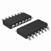
MC74HCT04ADR2G ON Semiconductor, MC74HCT04ADR2G Datasheet - Page 4

MC74HCT04ADR2G
Manufacturer Part Number
MC74HCT04ADR2G
Description
IC INVERTER HEX LSTTL IN 14-SOIC
Manufacturer
ON Semiconductor
Series
74HCTr
Datasheet
1.MC74HCT04ADTR2G.pdf
(8 pages)
Specifications of MC74HCT04ADR2G
Logic Type
Inverter
Number Of Inputs
1
Number Of Circuits
6
Current - Output High, Low
4mA, 4mA
Voltage - Supply
4.5 V ~ 5.5 V
Operating Temperature
-55°C ~ 125°C
Mounting Type
Surface Mount
Package / Case
14-SOIC (3.9mm Width), 14-SOL
Logical Function
Inverter
Logic Family
HCT
Number Of Elements
6
High Level Output Current
-4mA
Low Level Output Current
4mA
Propagation Delay Time
26ns
Operating Supply Voltage (typ)
5V
Package Type
SOIC
Operating Temp Range
-55C to 125C
Pin Count
14
Quiescent Current
1uA
Technology
CMOS
Mounting
Surface Mount
Operating Temperature Classification
Military
Operating Supply Voltage (max)
5.5V
Operating Supply Voltage (min)
4.5V
Lead Free Status / RoHS Status
Lead free / RoHS Compliant
Other names
MC74HCT04ADR2GOS
MC74HCT04ADR2GOS
MC74HCT04ADR2GOSTR
MC74HCT04ADR2GOS
MC74HCT04ADR2GOSTR
Available stocks
Company
Part Number
Manufacturer
Quantity
Price
Company:
Part Number:
MC74HCT04ADR2G
Manufacturer:
ON Semiconductor
Quantity:
20 000
3. For propagation delays with loads other than 50 pF, and information on typical parametric values, see Chapter 2 of the ON Semiconductor
* Used to determine the no−load dynamic power consumption: P
AC CHARACTERISTICS
Symbol
ON Semiconductor High−Speed CMOS Data Book (DL129/D).
t
t
t
C
t
OUTPUT Y
PLH
High−Speed CMOS Data Book (DL129/D).
TLH
PHL
THL
C
PD
in
INPUT A
,
,
Maximum Propagation Delay, Input A to Output Y
(Figures 1 and 2)
Maximum Output Transition Time, Any Output
(Figures 1 and 2)
Maximum Input Capacitance
Power Dissipation Capacitance (Per Inverter)*
2.7V
1.3V
0.3V
t
PLH
t
TLH
10%
Figure 1. Switching Waveforms
1.3V
90%
(V
CC
t
f
= 5.0V ±10%, C
t
r
Parameter
A
Figure 3. Expanded Logic Diagram
L
= 50pF, Input t
(1/6 of the Device Shown)
http://onsemi.com
t
PHL
D
r
= C
= t
4
t
THL
f
3.0V
GND
PD
= 6ns)
V
CC
2
f + I
CC
V
CC
−55 to 25°C
. For load considerations, see Chapter 2 of the
15
17
15
10
Typical @ 25°C, V
Y
*Includes all probe and jig capacitance
Guaranteed Limit
Figure 2. Test Circuit
DEVICE
UNDER
TEST
≤85°C
22
19
21
19
10
CC
= 5.0 V
OUTPUT
≤125°C
22
26
22
10
POINT
TEST
C
Unit
pF
pF
ns
ns
L
*


