MC14007UBFELG ON Semiconductor, MC14007UBFELG Datasheet
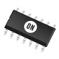
IC COMP DUAL PAIR W/INV 14SOEIAJ

MC14007UBFELG

Manufacturer Part Number
MC14007UBFELG
Description
IC COMP DUAL PAIR W/INV 14SOEIAJ
Manufacturer
ON Semiconductor
Series
4000Br
Datasheet

Specifications of MC14007UBFELG

Logic Type
Configurable Multiple Function
Number Of Circuits
2
Number Of Inputs
1
Schmitt Trigger Input
No
Output Type
Single-Ended
Current - Output High, Low
10mA, 10mA
Voltage - Supply
3 V ~ 18 V
Operating Temperature
-55°C ~ 125°C
Mounting Type
Surface Mount
Package / Case
14-SOIC (5.3mm Width), 14-SOP, 14-SOIJ
Logic Family
4000
Number Of Channels Per Chip
3
Polarity
Inverting
Supply Voltage (max)
18 V
Supply Voltage (min)
3 V
Maximum Operating Temperature
+ 125 C
Mounting Style
SMD/SMT
High Level Output Current
- 4.2 mA
Low Level Output Current
4.2 mA
Minimum Operating Temperature
- 55 C
Number Of Lines (input / Output)
3 / 3
Propagation Delay Time
125 ns at 5 V, 75 ns at 10 V, 55 ns at 15 V
Lead Free Status / RoHS Status
Lead free / RoHS Compliant
MC14007UB
Dual Complementary Pair
Plus Inverter
and three P−Channel enhancement mode devices packaged to provide
access to each device. These versatile parts are useful in inverter
circuits, pulse−shapers, linear amplifiers, high input impedance
amplifiers, threshold detectors, transmission gating, and functional
gating.
Features
Stresses exceeding Maximum Ratings may damage the device. Maximum
Ratings are stress ratings only. Functional operation above the Recommended
Operating Conditions is not implied. Extended exposure to stresses above the
Recommended Operating Conditions may affect device reliability.
1. Temperature Derating:
MAXIMUM RATINGS
© Semiconductor Components Industries, LLC, 2006
October, 2006 − Rev. 8
Symbol
V
I
The MC14007UB multipurpose device consists of three N−Channel
in
Schottky TTL Load Over the Rated Temperature Range
precautions must be taken.
in
Diode Protection on All Inputs
Supply Voltage Range = 3.0 Vdc to 18 Vdc
Capable of Driving Two Low−power TTL Loads or One Low−power
Pin−for−Pin Replacement for CD4007A or CD4007UB
This device has 2 outputs without ESD Protection. Antistatic
Pb−Free Packages are Available
V
T
Plastic “P and D/DW” Packages: – 7.0 mW/°C from 65°C 5o 125°C.
P
, V
, I
T
T
stg
DD
A
D
L
out
out
DC Supply Voltage Range
Input or Output Voltage Range
(DC or Transient)
Input or Output Current
(DC or Transient) per Pin
Power Dissipation, per Package
(Note 1)
Ambient Temperature Range
Storage Temperature Range
Lead Temperature
(8 second Soldering)
Parameter
(Voltages Referenced to V
−0.5 to V
−0.5 to +18.0
SS
−55 to +125
−65 to +150
)
Value
± 10
500
260
DD
+0.5
1
Unit
mW
mA
°C
°C
°C
V
V
See detailed ordering and shipping information in the package
dimensions section on page 6 of this data sheet.
GATE
GATE
ORDERING INFORMATION
A
WL, L
YY, Y
WW, W
G
D−P
S−N
D−N
S−P
V
SS
http://onsemi.com
PIN ASSIGNMENT
B
B
B
B
B
A
CASE 751A
SOEIAJ−14
S = SOURCE
CASE 646
CASE 965
D SUFFIX
P SUFFIX
F SUFFIX
1
2
3
4
5
6
7
SOIC−14
PDIP−14
D = DRAIN
= Assembly Location
= Wafer Lot
= Year
= Work Week
= Pb−Free Indicator
Publication Order Number:
14
13
12
10
11
9
8
14
1
14
14
1
1
V
D−P
OUT
S−P
GATE
S−N
D−N
MC14007UBCP
DIAGRAMS
AWLYYWWG
MC14007UB
DD
MARKING
MC14007UB/D
AWLYWW
14007UG
ALYWG
A
C
C
A
C
C

Related parts for MC14007UBFELG

MC14007UBFELG Summary of contents

Page 1

MC14007UB Dual Complementary Pair Plus Inverter The MC14007UB multipurpose device consists of three N−Channel and three P−Channel enhancement mode devices packaged to provide access to each device. These versatile parts are useful in inverter circuits, pulse−shapers, linear amplifiers, high input ...

Page 2

INPUT INPUT OUTPUT CONDITION INPUT OPEN OPEN Substrates of P−Channel devices internally connected substrates of N−Channel DD devices internally connected to V ...

Page 3

ELECTRICAL CHARACTERISTICS Î Î Î Î Î ...

Page 4

SWITCHING CHARACTERISTICS Î Î Î Î Î ...

Page 5

V DD 0.01 mF 500 mF I CERAMIC PULSE in GENERATOR Figure 5. Switching Time and Power Dissipation Test Circuit and Waveforms The MC14007UB dual pair plus inverter, which has access to all its ...

Page 6

... Device MC14007UBCP MC14007UBCPG MC14007UBD MC14007UBDG MC14007UBDR2 MC14007UBDR2G MC14007UBFEL MC14007UBFELG †For information on tape and reel specifications, including part orientation and tape sizes, please refer to our Tape and Reel Packaging Specifications Brochure, BRD8011/D. Package PDIP−14 PDIP−14 (Pb−Free) SOIC−14 SOIC−14 (Pb− ...

Page 7

−T− SEATING PLANE 0.13 (0.005) PACKAGE DIMENSIONS PDIP−14 CASE 646−06 ISSUE http://onsemi.com 7 NOTES: 1. DIMENSIONING AND TOLERANCING PER ANSI ...

Page 8

... G −T− SEATING 14 PL PLANE 0.25 (0.010 14X 0.58 *For additional information on our Pb−Free strategy and soldering details, please download the ON Semiconductor Soldering and Mounting Techniques Reference Manual, SOLDERRM/D. PACKAGE DIMENSIONS SOIC−14 CASE 751A−03 ISSUE 0.25 (0.010 ...

Page 9

... Opportunity/Affirmative Action Employer. This literature is subject to all applicable copyright laws and is not for resale in any manner. PUBLICATION ORDERING INFORMATION LITERATURE FULFILLMENT: Literature Distribution Center for ON Semiconductor P.O. Box 5163, Denver, Colorado 80217 USA Phone: 303−675−2175 or 800−344−3860 Toll Free USA/Canada Fax: 303− ...

Related keywords