MC74HCT373AN ON Semiconductor, MC74HCT373AN Datasheet

IC LATCH TRNSP OCTAL 3ST 20DIP

MC74HCT373AN

Manufacturer Part Number
MC74HCT373AN
Description
IC LATCH TRNSP OCTAL 3ST 20DIP
Manufacturer
ON Semiconductor
Series
74HCTr
Datasheet

Specifications of MC74HCT373AN

Logic Type
D-Type Transparent Latch
Circuit
8:8
Output Type
Tri-State
Voltage - Supply
4.5 V ~ 5.5 V
Independent Circuits
1
Delay Time - Propagation
28ns
Current - Output High, Low
6mA, 6mA
Operating Temperature
-55°C ~ 125°C
Mounting Type
Through Hole
Package / Case
20-DIP (0.300", 7.62mm)
Lead Free Status / RoHS Status
Contains lead / RoHS non-compliant
Other names
MC74HCT373ANOS
MC74HCT373A
Octal 3−State Noninverting
Transparent Latch with
LSTTL−Compatible Inputs
High−Performance Silicon−Gate CMOS
interfacing TTL or NMOS outputs to High−Speed CMOS inputs.
While the Latch Enable is high the Q outputs follow the Data Inputs.
When Latch Enable is taken low, data meeting the setup and hold
times becomes latched.
Output Enable is high, all outputs are forced to the high−impedance
state. Thus, data may be latched even when the outputs are not
enabled.
the input pins on the opposite side of the package from the output pins.
This device is similar in function to the HCT533A, which has
inverting outputs.
w
© Semiconductor Components Industries, LLC, 2006
March, 2006 − Rev. 11
The MC74HCT373A may be used as a level converter for
The HCT373A is identical in pinout to the LS373.
The eight latches of the HCT373A are transparent D−type latches.
The Output Enable does not affect the state of the latch, but when
The HCT373A is identical in function to the HCT573A, which has
No. 7A
These devices are available in Pb−free package(s). Specifications herein
apply to both standard and Pb−free devices. Please see our website at
www.onsemi.com for specific Pb−free orderable part numbers, or
contact your local ON Semiconductor sales office or representative.
Output Drive Capability: 15 LSTTL Loads
TTL/NMOS−Compatible Input Levels
Outputs Directly Interface to CMOS, NMOS, and TTL
Operating Voltage Range: 4.5 to 5.5 V
Low Input Current: 1.0 mA
In Compliance with the Requirements Defined by JEDEC Standard
Chip Complexity: 196 FETs or 49 Equivalent Gates
1
20
ORDERING INFORMATION
MC74HCT373AN
MC74HCT373ADW
MC74HCT373ADWR2 SOIC−WIDE
MC74HCT373ADT
MC74HCT373ADTR2
20
20
1
1
Device
1
A
WL = Wafer Lot
YY = Year
WW = Work Week
SOIC WIDE−20
http://onsemi.com
DW SUFFIX
CASE 751D
= Assembly Location
CASE 948E
TSSOP−20
DT SUFFIX
CASE 738
N SUFFIX
PDIP−20
SOIC−WIDE
Publication Order Number:
TSSOP−20
TSSOP−20
Package
PDIP−20
MC74HCT373A/D
20
MC74HCT373AN
20
1
1
DIAGRAMS
MARKING
AWLYYWW
AWLYYWW
20
HCT373A
1
1000 / Reel
2500 / Reel
1440 / Box
Shipping
38 / Rail
75 / Rail
ALYW
373A
HCT

Related parts for MC74HCT373AN

MC74HCT373AN Summary of contents

Page 1

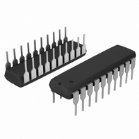
... CASE 948E A = Assembly Location WL = Wafer Lot YY = Year WW = Work Week ORDERING INFORMATION Device MC74HCT373AN MC74HCT373ADW MC74HCT373ADWR2 SOIC−WIDE MC74HCT373ADT MC74HCT373ADTR2 1 MARKING DIAGRAMS 20 MC74HCT373AN AWLYYWW 1 20 HCT373A AWLYYWW 1 20 HCT 373A ALYW 1 Package Shipping PDIP−20 1440 / Box SOIC−WIDE 38 / Rail 1000 / Reel TSSOP− ...

Page 2

LOGIC DIAGRAM DATA D3 INPUTS LATCH ENABLE 1 OUTPUT ENABLE Î Î Î Î Î Î Î Î Î Î Î Design Criteria Î ...

Page 3

... SOIC Package: – 7 mW/°C from 65° to 125°C TSSOP Package: − 6.1 mW/°C from 65° to 125°C For high frequency or heavy load considerations, see Chapter 2 of the ON Semiconductor High−Speed CMOS Data Book (DL129/D). RECOMMENDED OPERATING CONDITIONS Î Î Î Î ...

Page 4

... NOTE: 1. Total Supply Current = I CC NOTE: Information on typical parametric values can be found in Chapter 2 of the ON Semiconductor High−Speed CMOS Data Book (DL129/D). AC ELECTRICAL CHARACTERISTICS Î Î Î Î Î ...

Page 5

LATCH 11 ENABLE OUTPUT 1 ENABLE 2.7 V INPUT D 1 PLH 90% 1 10% t TLH Figure 1. OUTPUT ...

Page 6

TEST POINT OUTPUT DEVICE UNDER C * TEST L *Includes all probe and jig capacitance Figure 5. TEST CIRCUITS TEST POINT OUTPUT DEVICE UNDER TEST *Includes all probe and jig capacitance http://onsemi.com 6 CONNECT TO V WHEN ...

Page 7

SEATING PLANE 20X 0. 18X PACKAGE DIMENSIONS PDIP−20 N SUFFIX PLASTIC DIP PACKAGE CASE 738−03 ISSUE ...

Page 8

... N F DETAIL DETAIL E N. American Technical Support: 800−282−9855 Toll Free USA/Canada Japan: ON Semiconductor, Japan Customer Focus Center 2−9−1 Kamimeguro, Meguro−ku, Tokyo, Japan 153−0051 Phone: 81−3−5773−3850 http://onsemi.com 8 NOTES: 1. DIMENSIONING AND TOLERANCING PER ANSI Y14.5M, 1982. ...

Related keywords