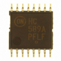
MC74HC589ADTR2G ON Semiconductor, MC74HC589ADTR2G Datasheet - Page 8

MC74HC589ADTR2G
Manufacturer Part Number
MC74HC589ADTR2G
Description
IC SHIFT REGISTER 8BIT 16-TSSOP
Manufacturer
ON Semiconductor
Series
74HCr
Datasheet
1.MC74HC589ADTR2G.pdf
(14 pages)
Specifications of MC74HC589ADTR2G
Logic Type
Shift Register
Output Type
Standard
Number Of Elements
1
Number Of Bits Per Element
8
Function
Universal
Voltage - Supply
2 V ~ 6 V
Operating Temperature
-55°C ~ 125°C
Mounting Type
Surface Mount
Package / Case
16-TSSOP
Lead Free Status / RoHS Status
Lead free / RoHS Compliant
Other names
MC74HC589ADTR2G
MC74HC589ADTR2GOSTR
MC74HC589ADTR2GOSTR
Available stocks
Company
Part Number
Manufacturer
Quantity
Price
Company:
Part Number:
MC74HC589ADTR2G
Manufacturer:
ON
Quantity:
1 000
Company:
Part Number:
MC74HC589ADTR2G
Manufacturer:
ON Semiconductor
Quantity:
74 238
Part Number:
MC74HC589ADTR2G
Manufacturer:
ON/安森美
Quantity:
20 000
Data Inputs
A, B, C, D, E, F, G, H (Pins 15, 1, 2, 3, 4, 5, 6, 7)
data latch on the rising edge of the Latch Clock input.
S
register on the rising edge of the Shift Clock input if Serial
Shift/Parallel Load is high. Data on this input is ignored
when Serial Shift/Parallel Load is low.
Control Inputs
Serial Shift/Parallel Load (Pin 13)
to this pin, the shift register is allowed to serially shift data.
When a low level is applied to this pin, the shift register
accepts parallel data from the data latch.
Shift Clock (Pin 11)
shifts data on the serial data input into the shift register and
A
Parallel data inputs. Data on these inputs are stored in the
Serial data input. Data on this input is shifted into the shift
Shift register mode control. When a high level is applied
Serial shift clock. A low-to-high transition on this input
(Pin 14)
CLOCK
LATCH
A-H
*Includes all probe and jig capacitance.
DEVICE
UNDER
TEST
Figure 10. Test Circuit
t
Figure 7.
50%
su
VALID
OUTPUT
DATA
50%
t
TEST POINT
SERIAL SHIFT/
h
PARALLEL
CLOCK
SHIFT
LOAD
C
L
*
Switching Waveforms
V
GND
CC
Pin Descriptions
http://onsemi.com
MC74HC589A
Figure 9.
t
su
50%
8
DEVICE
UNDER
TEST
data in stage H is shifted out Q
previously stored in stage G.
Latch Clock (Pin 12)
loads the parallel data on inputs A-H into the data latch.
Output Enable (Pin 10)
forces the Q
level enables the output. This control does not affect the state
of the input latch or the shift register.
Output
Q
of the shift register. This is a 3-state output.
50%
H
Data latch clock. A low-to-high transition on this input
Active-low output enable A high level applied to this pin
Serial data output. This pin is the output from the last stage
CLOCK
(Pin 9)
SHIFT
S
OUTPUT
*Includes all probe and jig capacitance.
A
TEST POINT
H
output into the high impedance state. A low
Figure 11. Test Circuit
C
V
GND
L
1 kW
CC
*
Figure 8.
t
50%
su
VALID
DATA
50%
H
t
, being replaced by the data
CONNECT TO V
TESTING t
CONNECT TO GND WHEN
TESTING t
h
PLZ
PHZ
AND t
AND t
CC
WHEN
V
GND
PZL
PZH
CC
.
.


