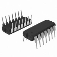
MC74HC164ANG ON Semiconductor, MC74HC164ANG Datasheet - Page 6

MC74HC164ANG
Manufacturer Part Number
MC74HC164ANG
Description
IC SHIFT REG 8BIT SER/PAR 14-DIP
Manufacturer
ON Semiconductor
Series
74HCr
Datasheet
1.MC74HC164ADG.pdf
(11 pages)
Specifications of MC74HC164ANG
Logic Type
Shift Register
Output Type
Standard
Number Of Elements
1
Number Of Bits Per Element
8
Function
Serial to Parallel
Voltage - Supply
2 V ~ 6 V
Operating Temperature
-55°C ~ 125°C
Mounting Type
Through Hole
Package / Case
14-DIP (0.300", 7.62mm)
Lead Free Status / RoHS Status
Lead free / RoHS Compliant
Other names
MC74HC164ANGOS
INPUTS
A1, A2 (Pins 1, 2)
to be entered into the first stage of the shift register. For a
high level to be entered into the shift register, both A1 and
A2 inputs must be high, thereby allowing one input to be
used as a data−enable input. When only one serial input is
used, the other must be connected to V
Clock (Pin 8)
pin shifts the data at each stage to the next stage. The shift
Serial Data Inputs. Data at these inputs determine the data
Shift Register Clock. A positive−going transition on this
CLOCK
A1 OR A2
Q
CLOCK
10%
50%
90%
10%
50%
90%
t
r
t
w
t
PLH
t
TLH
50%
Figure 1.
Figure 3.
t
su
1/f
max
VALID
t
PHL
t
f
50%
t
THL
CC
t
h
.
SWITCHING WAVEFORMS
PIN DESCRIPTIONS
GND
V
CC
http://onsemi.com
V
GND
V
GND
CC
CC
6
register is completely static, allowing clock rates down to
DC in a continuous or intermittent mode.
OUTPUTS
Q
presented at these outputs in true, or noninverted, form.
CONTROL INPUT
Reset (Pin 9)
applied to this input resets all internal flip−flops and sets
Outputs Q
A
Parallel Shift Register Outputs. The shifted data is
Active−Low, Asynchronous Reset Input. A low voltage
CLOCK
RESET
− Q
Q
H
(Pins 3, 4, 5, 6, 10, 11, 12, 13)
A
− Q
*Includes all probe and jig capacitance
t
H
PHL
to the low level state.
DEVICE
UNDER
Figure 4. Test Circuit
TEST
50%
Figure 2.
t
w
t
50%
rec
OUTPUT
50%
TEST POINT
C
L
*
V
GND
GND
V
CC
CC


