MC74VHC595DR2G ON Semiconductor, MC74VHC595DR2G Datasheet
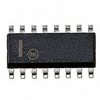
IC SHIFT REG 8BIT 3ST 16-SOIC

MC74VHC595DR2G

Manufacturer Part Number
MC74VHC595DR2G
Description
IC SHIFT REG 8BIT 3ST 16-SOIC
Manufacturer
ON Semiconductor
Series
74VHCr
Datasheet

Specifications of MC74VHC595DR2G

Logic Type
Shift Register
Output Type
Standard
Number Of Elements
1
Number Of Bits Per Element
8
Function
Serial to Parallel
Voltage - Supply
2 V ~ 5.5 V
Operating Temperature
-55°C ~ 125°C
Mounting Type
Surface Mount
Package / Case
16-SOIC (3.9mm Width)
Lead Free Status / RoHS Status
Lead free / RoHS Compliant

Available stocks

Company
Part Number
Manufacturer
Quantity
Price
Part Number:
MC74VHC595DR2G
Manufacturer:
ON Semiconductor
Quantity:
1 100
Part Number:
MC74VHC595DR2G
0
MC74VHC595
8-Bit Shift Register with
Output Storage Register
(3-State)
with an output storage register fabricated with silicon gate CMOS
technology.
Schottky TTL while maintaining CMOS low power dissipation.
feeds an 8-bit storage register.
the Shift Clock input (SCK). The output register is loaded with the
contents of the shift register on the positive going transition of the
Register Clock input (RCK). Since the RCK and SCK signals are
independent, parallel outputs can be held stable during the shift
operation. And, since the parallel outputs are 3-state, the VHC595 can
be directly connected to an 8-bit bus. This register can be used in
serial-to-parallel conversion, data receivers, etc.
output which provides high noise immunity and stable output. The
inputs tolerate voltages up to 7V, allowing the interface of 5V systems
to 3V systems.
Features
© Semiconductor Components Industries, LLC, 2007
September, 2007 - Rev. 5
The MC74VHC595 is an advanced high speed 8-bit shift register
It achieves high speed operation similar to equivalent Bipolar
The MC74VHC595 contains an 8-bit static shift register which
Shift operation is accomplished on the positive going transition of
The internal circuit is composed of three stages, including a buffer
High Speed: f
Low Power Dissipation: I
High Noise Immunity: V
Power Down Protection Provided on Inputs
Balanced Propagation Delays
Designed for 2V to 5.5V Operating Range
Low Noise: V
Pin and Function Compatible with Other Standard Logic Families
Latchup Performance Exceeds 300mA
ESD Performance: HBM > 2000V; Machine Model > 200V
These are Pb-Free Devices
max
OLP
= 185MHz (Typ) at V
= 1.0V (Max)
NIH
CC
= 4μA (Max) at T
= V
NIL
= 28% V
CC
= 5V
CC
A
= 25°C
1
†For information on tape and reel specifications,
MC74VHC595DR2G
MC74VHC595DTR2G TSSOP-16
including part orientation and tape sizes, please
refer to our Tape and Reel Packaging Specification
Brochure, BRD8011/D.
CASE 751B
CASE 948F
DT SUFFIX
TSSOP-16
D SUFFIX
(Note: Microdot may be in either location)
SOIC-16
Device
ORDERING INFORMATION
A
WL
Y
W, WW = Work Week
G or G
GND
QC
QG
QH
QB
QD
QE
QF
http://onsemi.com
PIN ASSIGNMENT
1
2
3
4
5
6
7
8
= Assembly Location
= Wafer Lot
= Year
= Pb-Free Package
MARKING DIAGRAMS
(Pb-Free)
(Pb-Free)
SOIC-16
Publication Order Number:
16
Package
1
16
1
10
16
15
14
13
12
11
9
VHC595G
AWLYWW
ALYWG
MC74VHC595/D
VHC
VCC
QA
SI
OE
RCK
SCK
SCLR
SQH
595
G
2500 Tape &
2500 Tape &
Shipping
Reel
Reel
9
8
8
9

Related parts for MC74VHC595DR2G

MC74VHC595DR2G Summary of contents

Page 1

... ESD Performance: HBM > 2000V; Machine Model > 200V • These are Pb-Free Devices © Semiconductor Components Industries, LLC, 2007 September, 2007 - Rev 25° 28 MC74VHC595DR2G MC74VHC595DTR2G TSSOP-16 †For information on tape and reel specifications, 1 http://onsemi.com MARKING DIAGRAMS 16 VHC595G AWLYWW SOIC- SUFFIX CASE 751B ...

Page 2

MC74VHC595 LOGIC DIAGRAM SERIAL 14 DATA SI INPUT SHIFT STORAGE REGISTER REGISTER 11 SCK 10 SCLR 12 RCK 13 OE IEC LOGIC SYMBOL 13 OE EN3 12 RSK C2 SRG8 10 R SCLR 11 SCK C ...

Page 3

OE 12 RCK SCK 10 SCLR MC74VHC595 EXPANDED LOGIC DIAGRAM SRA STRA SRB STRB SRC STRC SRD ...

Page 4

Reset (SCLR) Operation Clear shift register L Shift data into shift H register Registers remains H unchanged Transfer shift register H contents to storage register Storage register remains X unchanged Enable parallel outputs X Force outputs into high X impedance ...

Page 5

The q of the package is equal to 1/Derating. Higher junction temperatures may affect the expected lifetime of the device per the table and JA figure below. DEVICE JUNCTION TEMPERATURE VERSUS TIME TO 0.1% BOND FAILURES Junction Temperature °C Time, ...

Page 6

AC ELECTRICAL CHARACTERISTICS Î Î Î Î ...

Page 7

TIMING REQUIREMENTS (Input t Î Î Î Î Î Î Î Î Î Î Î Î Î Î Î Î Î Î Î Î Î Î Î Î Î Î Î Î Î Î Î Î Î Î Î Î ...

Page 8

SCK 50 1/f max t t PLH PHL SQH 50 Figure 2. RCK 50 PLH PHL QA-QH 50 Figure 4. SCLR 50% VALID 50 50% SCK or ...

Page 9

SCK SI SCLR RCK SQH NOTE: output high-impedance state. INPUT MC74VHC595 TIMING DIAGRAM INPUT EQUIVALENT CIRCUIT http://onsemi.com 9 ...

Page 10

... IDENT. 1 0.15 (0.006 -V- C 0.10 (0.004) -T- SEATING D PLANE 16X 0.36 *For additional information on our Pb-Free strategy and soldering details, please download the ON Semiconductor Soldering and Mounting Techniques Reference Manual, SOLDERRM/D. MC74VHC595 PACKAGE DIMENSIONS TSSOP-16 CASE 948F-01 ISSUE É É É Ç Ç Ç ...

Page 11

... *For additional information on our Pb-Free strategy and soldering details, please download the ON Semiconductor Soldering and Mounting Techniques Reference Manual, SOLDERRM/D. ON Semiconductor and are registered trademarks of Semiconductor Components Industries, LLC (SCILLC). SCILLC reserves the right to make changes without further notice to any products herein. SCILLC makes no warranty, representation or guarantee regarding the suitability of its products for any particular purpose, nor does SCILLC assume any liability arising out of the application or use of any product or circuit, and specifically disclaims any and all liability, including without limitation special, consequential or incidental damages. “ ...

Related keywords