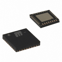
SY58026UMG Micrel Inc, SY58026UMG Datasheet - Page 2

SY58026UMG
Manufacturer Part Number
SY58026UMG
Description
IC MUX DUAL 2:1 DFF LVPECL 32MLF
Manufacturer
Micrel Inc
Series
SY58r
Type
Multiplexerr
Datasheet
1.SY58026UMG.pdf
(11 pages)
Specifications of SY58026UMG
Circuit
1 x 2:1
Independent Circuits
2
Voltage Supply Source
Single Supply
Voltage - Supply
3 V ~ 3.6 V
Operating Temperature
-40°C ~ 85°C
Mounting Type
Surface Mount
Package / Case
32-MLF®, QFN
Number Of Clock Inputs
4
Mode Of Operation
Differential
Output Frequency
6000MHz
Output Logic Level
LVPECL
Operating Supply Voltage (min)
2.375V
Operating Supply Voltage (typ)
2.5/3.3V
Operating Supply Voltage (max)
3.6V
Package Type
MLF
Operating Temp Range
-40C to 85C
Operating Temperature Classification
Industrial
Signal Type
CML/LVDS/PECL
Mounting
Surface Mount
Pin Count
32
Lead Free Status / RoHS Status
Lead free / RoHS Compliant
Current - Output High, Low
-
Lead Free Status / Rohs Status
Compliant
Other names
576-1383
M9999-082707
hbwhelp@micrel.com or (408) 955-1690
Micrel, Inc.
VREF-ACB0
VREF-ACB1
PACKAGE/ORDERING INFORMATION
PIN DESCRIPTION
Pin Number
26, 30, 2, 6
27, 31, 3, 7
10, 13, 16,
VTB0
/INB0
VTB1
/INB1
17, 20, 23
INB0
INB1
25, 28,
29, 32,
22, 21,
18, 15
12, 11
14, 19
32-Pin MLF
9, 24
1, 4,
5, 8
1
2
3
4
5
6
7
8
32 31 30 29 28 27 26 25
9 10 11 12 13 14 15 16
®
VTA0 , VTA1,
(MLF-32)
VREF-ACA0,
VREF-ACA1,
VREF-ACB0,
Exposed pad
SELA, SELB
VREF-ACB1
INA0, /INA0,
INA1, /INA1,
INB0, /INB0,
VTB0, VTB1
INB1, /INB1
Pin Name
QA, /QA,
QB, /QB
GND,
VCC
NC
24
23
22
21
20
19
18
17
GND
VCC
QA
/QA
VCC
NC
SELA
VCC
Pin Function
Differential Inputs: These input pairs are the differential signal inputs to the device. Inputs
accept AC- or DC-coupled differential signals as small as 100mV. Each pin of a pair internally
terminates to a VT pin through 50ý. Note that these inputs will default to an indeterminate
state if left open. Unused differential input pairs can be terminated by connecting one input
to V
left open in this configuration. Please refer to the “Input Interface Applications” section for
more details.
Input Termination Center-Tap: Each side of the differential input pair, terminates to a VT
pin. Each VT pin provides a center-tap to a termination network for maximum interface
flexibility. See “Input Interface Applications” section for more details.
Bank A, Bank B Input Channel Select (TTL/CMOS): These TTL/CMOS-compatible inputs
select the inputs to the multiplexers. These inputs are internally connected to a 25ký
pull-up resistor and will default to a logic HIGH state if left open. Input switching threshold
is V
Reference Output Voltage: These outputs bias to V
AC-coupling the data inputs. Bypass with 0.01µF low ESR capacitor to V
Maximum current source or sink is 0.5mA. See “Input Interface Applications” section.
Positive Power Supply: Bypass with 0.1µF™ℑ0.01µF low ESR capacitors.
Differential 100k LVPECL Outputs: MUX A and MUX B selected LVPECL outputs.
logic operation.
Ground: Ground pins and exposed pad must be connected to the same ground plane.
Not connected.
See “Output Interface Applications” section for termination. Refer to the “Truth Table” for
Ordering Information
Notes:
1. Contact factory for die availability. Dice are guaranteed at T
2. Tape and Reel.
CC
CC
Part Number
SY58026UMI
SY58026UMITR
SY58026UMG
SY58026UMGTR
/2.
and the complementary input to GND through a 1ký resistor. The VT pin is to be
(2)
(2)
2
Package
MLF-32
MLF-32
MLF-32
MLF-32
Type
(1)
Operating
Industrial
Industrial
Industrial
Industrial
Range
CC
Pb-Free bar-line indicator
Pb-Free bar-line indicator
–1.2V. Connect to VT pin when
SY58026U with
SY58026U with
A
SY58026U
SY58026U
= 25°C, DC electricals only.
Package
Marking
CC
.
Precision Edge
SY58026U
Pb-Free
Pb-Free
NiPdAu
NiPdAu
Finish
Sn-Pb
Sn-Pb
Lead
®


