ADG3247BRU-REEL7 Analog Devices Inc, ADG3247BRU-REEL7 Datasheet
ADG3247BRU-REEL7
Specifications of ADG3247BRU-REEL7


Related parts for ADG3247BRU-REEL7


ADG3247BRU-REEL7 Summary of contents
Page 1
FEATURES 225 ps Propagation Delay through the Switch 4.5 Switch Connection between Ports Data Rate 1.244 Gbps 2.5 V/3.3 V Supply Operation Selectable Level Shifting/Translation Small Signal Bandwidth 610 MHz Level Translation 3 2 ...
Page 2
ADG3247–SPECIFICATIONS Parameter DC ELECTRICAL CHARACTERISTICS Input High Voltage Input Low Voltage Input Leakage Current OFF State Leakage Current ON State Leakage Current Maximum Pass Voltage 3 CAPACITANCE A Port Off Capacitance B Port Off Capacitance A, B Port On Capacitance ...
Page 3
... Junction Temperature . . . . . . . . . . . . . . . . . . . . . . . . . . 150°C Model Temperature Range ADG3247BCP –40°C to +85°C ADG3247BCP-REEL7 –40°C to +85°C ADG3247BRU –40°C to +85°C ADG3247BRU-REEL7 –40°C to +85°C Table I. Pin Description Mnemonic Description BEx Bus Enable (Active Low) SEL Level Translation Select Ax ...
Page 4
ADG3247 V Positive Power Supply Voltage. CC GND Ground (0 V) Reference. V Minimum Input Voltage for Logic 1. INH V Maximum Input Voltage for Logic 0. INL I Input Leakage Current at the Control Inputs OFF State ...
Page 5
SEL = 3. 3. 0.5 1.0 1.5 2.0 2.5 3.0 3 ...
Page 6
ADG3247 3 2 2.0 = 3.3V; SEL = 1.5 = SEL = 3. 1.0 0.5 = SEL = 2. ...
Page 7
SEL = 3. p 20dB ATTENUATION EYE WIDTH = ((CLOCK PERIOD – 55 JITTER p-p)/CLOCK PERIOD) 100% 50 0.5 0.6 0.7 0.8 0.9 ...
Page 8
ADG3247 For the following load circuit and waveforms, the notation that is used OUT PULSE D.U.T. GENERATOR R T NOTES t PULSE GENERATOR FOR ALL PULSES: 2.5ns, R FREQUENCY 10MHz. C INCLUDES BOARD, ...
Page 9
BUS SWITCH APPLICATIONS Mixed Voltage Operation, Level Translation Bus switches can be used to provide an ideal solution for inter- facing between mixed voltage systems. The ADG3247 is suitable for applications where voltage translation from 3.3 V technology to a ...
Page 10
ADG3247 V OUT 3.3V SUPPLY SEL = 0V 1.8V SWITCH 0V 3.3V INPUT Figure 10. 3 1.8 V Voltage Translation, SEL = 0 V Bus Isolation A common requirement of bus architectures is low capacitance loading of the ...
Page 11
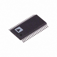
PIN 1 INDICATOR 12 MAX 1.00 0.90 0.80 SEATING PLANE 38-Lead Thin Shrink Small Outline Package [TSSOP] PIN 1 0.15 0.05 COPLANARITY REV. 0 OUTLINE DIMENSIONS 40-Lead Lead Frame Chip Scale Package [LFCSP] (CP-40) Dimensions shown in millimeters 6.00 BSC ...
Page 12
–12– ...