MC74VHC138DG ON Semiconductor, MC74VHC138DG Datasheet
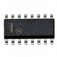
IC DECODER 1-8 ADV HS 16-SOIC

MC74VHC138DG

Manufacturer Part Number
MC74VHC138DG
Description
IC DECODER 1-8 ADV HS 16-SOIC
Manufacturer
ON Semiconductor
Series
74VHCr
Type
Decoderr
Datasheets

Specifications of MC74VHC138DG

Circuit
1 x 3:8
Independent Circuits
1
Current - Output High, Low
8mA, 8mA
Voltage Supply Source
Single Supply
Voltage - Supply
2 V ~ 5.5 V
Operating Temperature
-55°C ~ 125°C
Mounting Type
Surface Mount
Package / Case
16-SOIC (3.9mm Width)
Logic Type
Decoder / Demultiplexer
No. Of Outputs
8
Supply Voltage Range
2V To 5.5V
Logic Case Style
SOIC
No. Of Pins
16
Operating Temperature Range
-55°C To +125°C
Filter Terminals
SMD
Rohs Compliant
Yes
Family Type
VHC
Lead Free Status / RoHS Status
Lead free / RoHS Compliant

Available stocks

Company
Part Number
Manufacturer
Quantity
Price
Part Number:
MC74VHC138DG
Manufacturer:
ON Semiconductor
Quantity:
2
MC74VHC138
3- -to- -8 Line Decoder
decoder fabricated with silicon gate CMOS technology. It achieves
high speed operation similar to equivalent Bipolar Schottky TTL
while maintaining CMOS low power dissipation.
determine which one of the outputs (Y0 - - Y7) will go Low. When
enable input E3 is held Low or either E2 or E1 is held High, decoding
function is inhibited and all outputs go high. E3, E2, and E1 inputs are
provided to ease cascade connection and for use as an address decoder
for memory systems.
output which provides high noise immunity and stable output. The
inputs tolerate voltages up to 7V, allowing the interface of 5V systems
to 3V systems.
© Semiconductor Components Industries, LLC, 2006
March, 2006 - - Rev. 4
The MC74VHC138 is an advanced high speed CMOS 3- -to- -8
When the device is enabled, three Binary Select inputs (A0 - - A2)
The internal circuit is composed of three stages, including a buffer
These devices are available in Pb- -free package(s). Specifications herein
apply to both standard and Pb- -free devices. Please see our website at
www.onsemi.com for specific Pb- -free orderable part numbers, or
contact your local ON Semiconductor sales office or representative.
High Speed: t
Low Power Dissipation: I
High Noise Immunity: V
Power Down Protection Provided on Inputs
Balanced Propagation Delays
Designed for 2V to 5.5V Operating Range
Low Noise: V
Pin and Function Compatible with Other Standard Logic Families
Latchup Performance Exceeds 300mA
ESD Performance: HBM > 2000V; Machine Model > 200V
Chip Complexity: 122 FETs or 30.5 Equivalent Gates
PD
OLP
= 5.7ns (Typ) at V
= 0.8 V (Max)
NIH
CC
= 4μA (Max) at T
= V
NIL
CC
= 28% V
= 5V
CC
A
= 25°C
1
A
WL = Wafer Lot
Y
WW = Work Week
MC74VHC138D
MC74VHC138DR2
MC74VHC138DT
MC74VHC138DTR2 TSSOP--16 2500 Units/Reel
MC74VHC138M
MC74VHC138MEL
SOIC EIAJ- -16
Device
CASE 751B
CASE 948F
DT SUFFIX
TSSOP- -16
CASE 966
D SUFFIX
M SUFFIX
= Assembly Location
= Year
SOIC- -16
ORDERING INFORMATION
A
WL = Wafer Lot
YY = Year
WW = Work Week
http://onsemi.com
= Assembly Location
TSSOP--16
Package
SOIC--16
SOIC--16
EIAJ--16
EIAJ--16
MARKING DIAGRAMS
16
1
SOIC
SOIC
Publication Order Number:
16
16
1
1
A = Assembly Location
L = Wafer Lot
Y = Year
W = Work Week
AWLYWW
AWLYYWW
VHC138
VHC138
VHC
MC74VHC138/D
138
ALYW
2500 Units/Reel
2000 Units/Reel
48 Units/Rail
96 Units/Rail
48 Units/Rail
Shipping
9
8
8
9
8
9

Related parts for MC74VHC138DG

MC74VHC138DG Summary of contents

Page 1

... These devices are available in Pb- -free package(s). Specifications herein apply to both standard and Pb- -free devices. Please see our website at www.onsemi.com for specific Pb- -free orderable part numbers, or contact your local ON Semiconductor sales office or representative. © Semiconductor Components Industries, LLC, 2006 March, 2006 - - Rev. 4 ...

Page 2

PIN ASSIGNMENT GND 8 FUNCTION TABLE Inputs Outputs ...

Page 3

EXPANDED LOGIC DIAGRAM IEC LOGIC DIAGRAM BIN/OCT ...

Page 4

MAXIMUM RATINGS* Symbol Parameter V DC Supply Voltage Input Voltage Output Voltage out I Input Diode Current IK I Output Diode Current Output Current, per Pin out I DC Supply Current, ...

Page 5

DC ELECTRICAL CHARACTERISTICS Symbol Parameter Test Conditions V Minimum High--Level IH Input Voltage V Maximum IL Low--Level Input Voltage V Minimum High--Level Output Voltage μ ...

Page 6

VALID VALID A 50 PLH PHL Y 50 Figure 50% t PHL 50 Figure 4. INPUT SWITCHING WAVEFORMS GND t PHL GND t ...

Page 7

-T- - SEATING PLANE 0.25 (0.010 16X REF 0.10 (0.004) 0.15 (0.006 L PIN 1 IDENT. 1 ...

Page 8

... DETAIL P VIEW American Technical Support: 800--282--9855 Toll Free USA/Canada Japan: ON Semiconductor, Japan Customer Focus Center 2--9--1 Kamimeguro, Meguro--ku, Tokyo, Japan 153--0051 Phone: 81--3--5773--3850 http://onsemi.com 8 NOTES: 1. DIMENSIONING AND TOLERANCING PER ANSI Y14.5M, 1982. 2. CONTROLLING DIMENSION: MILLIMETER. ...

Related keywords