74F257APC Fairchild Semiconductor, 74F257APC Datasheet - Page 2
74F257APC
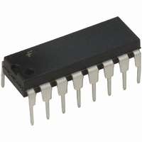
Manufacturer Part Number
74F257APC
Description
IC MULTIPLEXER QUAD 2INP 16-DIP
Manufacturer
Fairchild Semiconductor
Series
74Fr
Type
Multiplexerr
Datasheet
1.74F257APC.pdf
(7 pages)
Specifications of 74F257APC
Circuit
4 x 2:1
Independent Circuits
1
Current - Output High, Low
3mA, 24mA
Voltage Supply Source
Single Supply
Voltage - Supply
4.5 V ~ 5.5 V
Operating Temperature
0°C ~ 70°C
Mounting Type
Through Hole
Package / Case
16-DIP (0.300", 7.62mm)
Lead Free Status / RoHS Status
Lead free / RoHS Compliant
Other names
74F257
74F257PC
74F257PC
Available stocks
Company
Part Number
Manufacturer
Quantity
Price

Part Number:
74F257APC
Manufacturer:
NS/国半
Quantity:
20 000


www.fairchildsemi.com
Unit Loading/Fan Out
Truth Table
H
L
X
Z
Logic Diagram
Please note that this diagram is provided only for the understanding of logic operations and should not be used to estimate propagation delays.
LOW Voltage Level
High Impedance
HIGH Voltage Level
Immaterial
Output
Enable
OE
H
L
L
L
L
S
OE
I
I
Z
0a
1a
Pin Names
a
–Z
–I
–I
0d
1d
d
Select
Input
S
X
H
H
L
L
Common Data Select Input
3-STATE Output Enable Input (Active LOW)
Data Inputs from Source 0
Data Inputs from Source 1
3-STATE Multiplexer Outputs
I
X
X
X
H
L
0
Inputs
Data
I
H
X
L
X
X
1
Description
Output
H
H
Z
Z
L
L
2
Functional Description
The 74F257A is a quad 2-input multiplexer with 3-STATE
outputs. It selects four bits of data from two sources under
control of a Common Data Select input. When the Select
input is LOW, the I
is HIGH, the I
selected inputs appears at the outputs in true (non-
inverted) form. The device is the logic implementation of a
4-pole, 2-position switch where the position of the switch is
determined by the logic levels supplied to the Select input.
The logic equation for the outputs is shown below:
When the Output Enable input (OE) is HIGH, the outputs
are forced to a high impedance OFF state. If the outputs
are tied together, all but one device must be in the high
impedance state to avoid high currents that would exceed
the maximum ratings. Designers should ensure the Output
Enable signals to 3-STATE devices whose outputs are tied
together are designed so there is no overlap.
150/40 (33.3)
Z
HIGH/LOW
n
1.0/1.0
1.0/1.0
1.0/1.0
1.0/1.0
U.L.
1x
OE • (I
inputs are selected. The data on the
0x
inputs are selected and when Select
n
• S
3 mA/24 mA (20 mA)
I
on
Output I
20 A/ 0.6 mA
20 A/ 0.6 mA
20 A/ 0.6 mA
20 A/ 0.6 mA
Input I
• S)
IH
OH
/I
/I
IL
OL
Related parts for 74F257APC
Image
Part Number
Description
Manufacturer
Datasheet
Request
R

Part Number:
Description:
IC DECODER/DEMUX 1-OF-8 16-SOIC
Manufacturer:
Fairchild Semiconductor
Datasheet:
Part Number:
Description:
IC DECODER/DEMUX DL 1OF4 16-SOIC
Manufacturer:
Fairchild Semiconductor
Part Number:
Description:
IC MULTIPLEXER QUAD 2INP 16-SOIC
Manufacturer:
Fairchild Semiconductor
Datasheet:

Part Number:
Description:
IC DECODER/DEMUX 3/8LINE 16-DIP
Manufacturer:
Fairchild Semiconductor
Datasheet:
Part Number:
Description:
MULTIPLEXER QUAD 2INPUT 16SOIC
Manufacturer:
Fairchild Semiconductor
Datasheet:
Part Number:
Description:
DECODER/DEMUX 1-OF-8 16SOIC
Manufacturer:
Fairchild Semiconductor
Datasheet:

Part Number:
Description:
MULTIPLEXER QUAD 2INPUT 16SOP
Manufacturer:
Fairchild Semiconductor
Datasheet:
Part Number:
Description:
DECODER/DEMUX 1-OF-8 16SOP
Manufacturer:
Fairchild Semiconductor
Datasheet:
Part Number:
Description:
DECODER/DEMUX DUAL 1-OF-4 16SOP
Manufacturer:
Fairchild Semiconductor
Datasheet:
Part Number:
Description:
MULTIPLEXER QUAD 2INPUT 16SOP
Manufacturer:
Fairchild Semiconductor
Datasheet:

Part Number:
Description:
IC DECODER/DEMUX DUAL 2/4 16-DIP
Manufacturer:
Fairchild Semiconductor
Datasheet:
Part Number:
Description:
DECODER/DEMUX 1-OF-8 16SOP
Manufacturer:
Fairchild Semiconductor
Datasheet:
Part Number:
Description:
DECODER/DEMUX DUAL 1-OF-4 16SOP
Manufacturer:
Fairchild Semiconductor
Datasheet:

Part Number:
Description:
IC DECODER/DEMUX 3-8LINE 16SOIC
Manufacturer:
NXP Semiconductors
Datasheet:

Part Number:
Description:
IC DECODER/DEMUX 3-8LINE 16DIP
Manufacturer:
NXP Semiconductors
Datasheet: