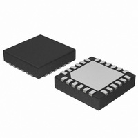
NB100LVEP56MNR2 ON Semiconductor, NB100LVEP56MNR2 Datasheet - Page 6

NB100LVEP56MNR2
Manufacturer Part Number
NB100LVEP56MNR2
Description
IC MUX DUAL 2:1 DIFF ECL 24QFN
Manufacturer
ON Semiconductor
Series
100LVEPr
Type
Differential Digital Multiplexerr
Datasheet
1.NB100LVEP56DTR2.pdf
(10 pages)
Specifications of NB100LVEP56MNR2
Circuit
2 x 2:1
Independent Circuits
1
Voltage Supply Source
Dual Supply
Voltage - Supply
2.38 V ~ 3.8 V
Operating Temperature
-40°C ~ 85°C
Mounting Type
Surface Mount
Package / Case
24-TFQFN Exposed Pad
Lead Free Status / RoHS Status
Contains lead / RoHS non-compliant
Current - Output High, Low
-
Other names
NB100LVEP56MNOSCT
NOTE: Device will meet the specifications after thermal equilibrium has been established when mounted in a test socket or printed circuit
14. Measured using a 750 mV source, 50% duty cycle clock source. All loading with 50 W to V
15. Pulse Skew |t
16. Worst case difference between D0a and D0b (or between D1a or D1b), when both output come from same input.
17. Worst case difference between Q0 and Q1 outputs.
18. Skew is measured between outputs under identical transitions.
19. Additive RMS jitter with 50% Duty Cycle Clock Signal.
20. Additive Peak−to−Peak jitter with input NRZ data at PRBS 2
21. Input voltage swing is a single−ended measurement operating in differential mode.
Table 8. AC CHARACTERISTICS
Symbol
V
t
t
t
t
V
t
t
PLH
PHL
Skew
JITTER
r
f
OUTPP
INPP
,
board with maintained transverse airflow greater than 500 lfpm. Electrical parameters are guaranteed only over the declared
operating temperature range. Functional operation of the device exceeding these conditions is not implied. Device specification limit
values are applied individually under normal operating conditions and not valid simultaneously.
Output Voltage Amplitude
(See Figure 4)
Propagation Delay to Output Differential
Pulse Skew (Note 15)
Within Device Input Skew (Note 16)
Within Device Output Skew (Note 17)
Device−to−Device Skew (Note 18)
RMS Random Clock Jitter (Note 19)
Peak−to−Peak Data Dependent Jitter (Note 20)
Input Voltage Swing (Differential Configuration)
(Note 21)
Output Rise/Fall Times @ 50 MHz
(20% − 80%)
PLH
− t
PHL
850
750
650
550
450
350
250
|
Characteristic
0.5
Figure 4. Output Voltage Amplitude (V
V
CC
COM_SEL to Q, Q
Q AMP (mV)
Input Frequency (f
= 0 V; V
@ 2.488 GHz
@ v1.0 GHz
@ v1.5 GHz
@ v2.0 GHz
@ v2.5 GHz
1.0
f
@ 1.25 GHz
in
SEL to Q, Q
f
in
@ 0.5 GHz
f
in
= 2.5 GHz
D to Q, Q
v 1 GHz
= 2 GHz
EE
INPUT FREQUENCY (GHz)
= −2.375 V to −3.8 V or V
Q, Q
http://onsemi.com
31
Min
525
500
400
375
575
550
150
60
−1.
1.5
in
6
) at V
−40°C
0.269
0.306
0.250
0.339
32.2
30.8
Typ
700
600
500
500
775
750
800
110
4.1
10
15
50
5
CC
= 2.5 V, 255C
1200
Max
625
975
950
200
150
0.4
0.4
0.4
0.8
50
30
50
16
80
66
CC
2.0
= 2.375 V to 3.8 V; V
OUTPP
Min
550
500
350
400
625
600
150
60
CC
) vs.
− 2.0 V. Input edge rates 150 ps (20% − 80%).
0.307
0.303
0.305
0.895
25°C
22.6
27.2
Typ
700
600
450
525
825
800
800
120
4.6
10
15
50
5
2.5
1025
1000
1200
Max
650
170
0.4
0.4
0.5
2.0
15
63
56
EE
= 0 V (Note 14)
Min
500
400
200
450
700
700
150
90
0.371
0.391
0.722
2.443
85°C
24.4
Typ
700
500
300
575
900
900
800
140
4.4
10
15
50
22
5
1200
1100
1100
Max
700
200
230
0.5
0.6
1.2
7.7
50
30
50
16
53
54
Unit
mV
mV
ps
ps
ps
ps


