MC14028BD ON Semiconductor, MC14028BD Datasheet
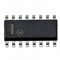
IC DECODER BCD-DECIMAL 16-SOIC

MC14028BD

Manufacturer Part Number
MC14028BD
Description
IC DECODER BCD-DECIMAL 16-SOIC
Manufacturer
ON Semiconductor
Series
4000Br
Type
Decoderr
Datasheet

Specifications of MC14028BD

Circuit
1 x 4:10
Independent Circuits
1
Voltage Supply Source
Dual Supply
Voltage - Supply
3 V ~ 18 V
Operating Temperature
-55°C ~ 125°C
Mounting Type
Surface Mount
Package / Case
16-SOIC (3.9mm Width)
Lead Free Status / RoHS Status
Contains lead / RoHS non-compliant
Current - Output High, Low
-

Available stocks

Company
Part Number
Manufacturer
Quantity
Price
Part Number:
MC14028BDG
Manufacturer:
ON/安森美
Quantity:
20 000
Part Number:
MC14028BDR2G
Manufacturer:
ON/安森美
Quantity:
20 000
MC14028B
BCD−To−Decimal Decoder
Binary−To−Octal Decoder
on the four inputs provides a decimal (one−of−ten) decoded output,
while a 3−bit binary input provides a decoded octal (one−of−eight)
code output with D forced to a logic “0”. Expanded decoding such as
binary−to−hexadecimal (one−of−sixteen), etc., can be achieved by
using other MC14028B devices. The part is useful for code
conversion, address decoding, memory selection control,
demultiplexing, or readout decoding.
Features
Stresses exceeding Maximum Ratings may damage the device. Maximum
Ratings are stress ratings only. Functional operation above the Recommended
Operating Conditions is not implied. Extended exposure to stresses above the
Recommended Operating Conditions may affect device reliability.
1. Temperature Derating: Plastic “P and D/DW”
static voltages or electric fields. However, precautions must be taken to avoid
applications of any voltage higher than maximum rated voltages to this
high−impedance circuit. For proper operation, V
to the range V
(e.g., either V
*For additional information on our Pb−Free strategy and soldering details, please
MAXIMUM RATINGS
© Semiconductor Components Industries, LLC, 2006
June, 2006 − Rev. 6
DC Supply Voltage Range
Input or Output Voltage Range
(DC or Transient)
Input or Output Current (DC or Transient)
per Pin
Power Dissipation per Package (Note 1)
Ambient Temperature Range
Storage Temperature Range
Lead Temperature (8−Second Soldering)
download the ON Semiconductor Soldering and Mounting Techniques
Reference Manual, SOLDERRM/D.
The MC14028B decoder is constructed so that an 8421 BCD code
This device contains protection circuitry to guard against damage due to high
Unused inputs must always be tied to an appropriate logic voltage level
Schottky TTL Load Over the Rated Temperature Range
Diode Protection on All Inputs
Supply Voltage Range = 3.0 Vdc to 18 Vdc
Capable of Driving Two Low−power TTL Loads or One Low−Power
Positive Logic Design
Low Outputs on All Illegal Input Combinations
Similar to CD4028B
Pb−Free Packages are Available*
Packages: – 7.0 mW/_C From 65_C To 125_C
SS
SS
Parameter
or V
v (V
DD
in
). Unused outputs must be left open.
or V
(Voltages Referenced to V
out
) v V
DD
.
Symbol
V
I
in
in
in
V
T
P
T
, V
, I
T
and V
DD
stg
D
A
L
out
out
SS
out
)
−0.5 to +18.0
−55 to +125
−65 to +150
−0.5 to V
should be constrained
Value
+ 0.5
± 10
500
260
DD
1
Unit
mW
mA
°C
°C
°C
V
V
See detailed ordering and shipping information in the package
dimensions section on page 2 of this data sheet.
1
1
1
ORDERING INFORMATION
A
WL, L
YY, Y
WW, W = Work Week
G
http://onsemi.com
CASE 751B
SOEIAJ−16
CASE 648
CASE 966
P SUFFIX
D SUFFIX
F SUFFIX
SOIC−16
= Assembly Location
= Wafer Lot
= Year
= Pb−Free Package
PDIP−16
Publication Order Number:
16
16
16
1
1
1
DIAGRAMS
MC14028BCP
AWLYYWWG
MARKING
MC14028B
AWLYWW
14028BG
MC14028B/D
ALYWG

Related parts for MC14028BD

MC14028BD Summary of contents

Page 1

... Unused inputs must always be tied to an appropriate logic voltage level (e.g., either Unused outputs must be left open *For additional information on our Pb−Free strategy and soldering details, please download the ON Semiconductor Soldering and Mounting Techniques Reference Manual, SOLDERRM/D. © Semiconductor Components Industries, LLC, 2006 June, 2006 − Rev Symbol ...

Page 2

... ORDERING INFORMATION Device MC14028BCP MC14028BCPG MC14028BD MC14028BDG MC14028BDR2 MC14028BDR2G MC14028BF MC14028BFEL MC14028BFELG †For information on tape and reel specifications, including part orientation and tape sizes, please refer to our Tape and Reel Packaging Specifications Brochure, BRD8011/D. MC14028B BLOCK DIAGRAM 10 A 3−BIT BINARY 13 B 8421 ...

Page 3

ELECTRICAL CHARACTERISTICS Î Î Î Î Î ...

Page 4

Inputs B, C, and D switching INPUT A in respect to a BCD code. INPUT C Inputs A, B, and D low APPLICATIONS INFORMATION Expanded decoding can be performed by using the MC14028B and other ...

Page 5

Inputs ...

Page 6

0.25 (0.010) M −A− −B− −T− SEATING PLANE 0.25 (0.010 MC14028B PACKAGE DIMENSIONS ...

Page 7

... Opportunity/Affirmative Action Employer. This literature is subject to all applicable copyright laws and is not for resale in any manner. PUBLICATION ORDERING INFORMATION LITERATURE FULFILLMENT: Literature Distribution Center for ON Semiconductor P.O. Box 5163, Denver, Colorado 80217 USA Phone: 303−675−2175 or 800−344−3860 Toll Free USA/Canada Fax: 303− ...

Related keywords