MC10H330FNG ON Semiconductor, MC10H330FNG Datasheet

IC DRIVER/RCVR QUAD BUS 28-PLCC

MC10H330FNG

Manufacturer Part Number
MC10H330FNG
Description
IC DRIVER/RCVR QUAD BUS 28-PLCC
Manufacturer
ON Semiconductor
Series
10Hr
Datasheet

Specifications of MC10H330FNG

Logic Type
Driver/Receiver
Number Of Bits
4
Operating Temperature
0°C ~ 75°C
Mounting Type
Surface Mount
Package / Case
28-PLCC
Logic Family
10H
Supply Voltage (min)
8 V
Maximum Operating Temperature
5 C
Mounting Style
SMD/SMT
Minimum Operating Temperature
0 C
Supply Current
157 mA
Lead Free Status / RoHS Status
Lead free / RoHS Compliant
Supply Voltage
-
Lead Free Status / Rohs Status
 Details

Available stocks

Company
Part Number
Manufacturer
Quantity
Price
Part Number:
MC10H330FNG
Manufacturer:
ON Semiconductor
Quantity:
135
Part Number:
MC10H330FNG
Manufacturer:
ON Semiconductor
Quantity:
10 000
MC10H330
Quad Bus Driver/Receiver
with 2−to−1 Output
Multiplexers
Description
output multiplexers. These multiplexers have a common select and
output enable. When disabled, (OE = high) the bus outputs go to
−2.0 V. Their output can be brought to a low state (V
high level to the receiver enable (RE = High). The parameters
specified are with 25 W loading on the bus drivers and 50 W loads on
the receivers.
Features
*For additional information on our Pb−Free strategy and soldering details, please
© Semiconductor Components Industries, LLC, 2006
February, 2006 − Rev. 7
download the ON Semiconductor Soldering and Mounting Techniques
Reference Manual, SOLDERRM/D.
The MC10H330 is a Quad Bus Driver/Receiver with two−to−one
Temperature Range)
Propagation Delay, 1.5 ns Typical Data−to−Output
Improved Noise Margin 150 mV (Over Operating Voltage and
Voltage Compensated
MECL 10K™ Compatible
Pb−Free Packages are Available*
For PLCC pin assignment, see the Pin Conversion Tables on page 18
of the ON Semiconductor MECL Data Book (DL122/D).
Pin assignment is for Dual−in−Line Package.
W
X
V
V
V
BUS
BUS
W
CC0
W1
W0
X
X1
X0
CC
EE
IN
IN
S
PIN ASSIGNMENT
2
3
4
5
6
7
8
10
11
12
1
9
DIP
19
24
23
22
21
20
18
17
16
15
14
13
V
Y
Z
OE
Y0
Y1
Z0
Z1
RE
Z
Y
VCC0
BUS
IN
CC0
BUS
IN
OL
) by applying a
1
See detailed ordering and shipping information in the package
dimensions section on page 3 of this data sheet.
CASE 758
CASE 724
CASE 776
L SUFFIX
P SUFFIX
P SUFFIX
PLCC−28
CDIP−24
PDIP−24
A
WL
YY
WW
G
ORDERING INFORMATION
http://onsemi.com
= Assembly Location
= Wafer Lot
= Year
= Work Week
= Pb−Free Package
MARKING DIAGRAMS*
Publication Order Number:
24
24
1
1
AWLYYWWG
MC10H330L
MC10H330P
AWLYYWW
AWLYYWW
10H330G
1
MC10H330/D

Related parts for MC10H330FNG

MC10H330FNG Summary of contents

Page 1

... For PLCC pin assignment, see the Pin Conversion Tables on page 18 of the ON Semiconductor MECL Data Book (DL122/D). *For additional information on our Pb−Free strategy and soldering details, please download the ON Semiconductor Soldering and Mounting Techniques Reference Manual, SOLDERRM/D. © Semiconductor Components Industries, LLC, 2006 February, 2006 − ...

Page 2

Table 1. MAXIMUM RATINGS Symbol V Power Supply ( Input Voltage ( Output Current − Continuous out − Surge T Operating Temperature Range A T Storage Temperature Range − Plastic ...

Page 3

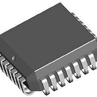
... RE 16 MULTIPLEXER TRUTH TABLE Bus Bus H X −2.0 V −2.0 V −2 ORDERING INFORMATION Device MC10H330FN MC10H330FNG MC10H330FNR2 MC10H330FNR2G MC10H330L MC10H330P MC10H330PG LOGIC DIAGRAM Z RE Bus Bus H −2 Package PLCC−28 PLCC−28 (Pb−Free) PLCC−28 PLCC−28 (Pb−Free) CDIP−24 PDIP−24 PDIP− ...

Page 4

0.010 (0.250) T L− NOTES: 1. DATUMS −L−, −M−, AND −N− DETERMINED WHERE TOP OF LEAD SHOULDER EXITS PLASTIC BODY AT MOLD ...

Page 5

... American Technical Support: 800−282−9855 Toll Free USA/Canada Japan: ON Semiconductor, Japan Customer Focus Center 2−9−1 Kamimeguro, Meguro−ku, Tokyo, Japan 153−0051 Phone: 81−3−5773−3850 http://onsemi.com 5 NOTES: 1. DIMENSIONING AND TOLERANCING PER ANSI Y14.5M, 1982. 2. CONTROLLING DIMENSION: INCH. ...

Related keywords