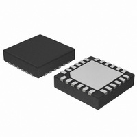
NB100LVEP17MN ON Semiconductor, NB100LVEP17MN Datasheet

NB100LVEP17MN
Specifications of NB100LVEP17MN
Available stocks
Related parts for NB100LVEP17MN
NB100LVEP17MN Summary of contents
Page 1
NB100LVEP17 2.5V / 3.3V Quad Differential Driver/Receiver Description The NB100LVEP17 is a 4-bit differential line receiver. The design incorporates two stages of gain, internal to the device, making it an excellent choice for use in high bandwidth amplifier applications. The ...
Page 2
Table 1. PIN DESCRIPTION Pin Á Á Á Á Á Á Á Á Á TSSOP QFN Name Á Á Á Á Á Á Á Á Á 1,20 13,18,21 22, 2,4,6,8 ...
Page 3
NB100LVEP17 Figure 2. TSSOP−20 ...
Page 4
Table 3. MAXIMUM RATINGS Symbol Parameter V Positive Mode Power Supply CC V Negative Mode Power Supply EE V Positive Mode Input Voltage I Negative Mode Input Voltage I Output Current out I V Sink/Source Operating Temperature ...
Page 5
Table 5. DC CHARACTERISTICS, PECL Symbol Characteristic I Negative Power Supply Current EE V Output HIGH Voltage (Note Output LOW Voltage (Note Input HIGH Voltage (Single−Ended Input LOW Voltage (Single−Ended ...
Page 6
Table 7. AC CHARACTERISTICS V Symbol Characteristic V Output Voltage Amplitude OUTPP (See Figures Propagation Delay to Output Differential PLH t PHL t Pulse Skew (Note 15) Skew Within Device Skew (Note 17) Device−to−Device Skew (Note ...
Page 7
Q AMP (mV) 650 550 450 350 RMS JITTER (ps) 250 0.5 1.0 1.5 INPUT FREQUENCY (GHz) Figure 4. Output Voltage Amplitude (V Input Frequency ( 2.5 V, Ambient Temperature in CC 850 750 ...
Page 8
... NB100LVEP17DT NB100LVEP17DTG NB100LVEP17DTR2 NB100LVEP17DTR2G NB100LVEP17MN NB100LVEP17MNG NB100LVEP17MNR2 NB100LVEP17MNR2G †For information on tape and reel specifications, including part orientation and tape sizes, please refer to our Tape and Reel Packaging Specification Brochure, BRD8011/D. *This package is inherently Pb−Free. Resource Reference of Application Notes AN1405/D AN1406/D AN1503/D ...
Page 9
... −V− 0.100 (0.004) −T− SEATING PLANE 16X 0.36 *For additional information on our Pb−Free strategy and soldering details, please download the ON Semiconductor Soldering and Mounting Techniques Reference Manual, SOLDERRM/D. PACKAGE DIMENSIONS TSSOP−20 CASE 948E−02 ISSUE Í Í Í Í ...
Page 10
... Opportunity/Affirmative Action Employer. This literature is subject to all applicable copyright laws and is not for resale in any manner. PUBLICATION ORDERING INFORMATION LITERATURE FULFILLMENT: Literature Distribution Center for ON Semiconductor P.O. Box 5163, Denver, Colorado 80217 USA Phone: 303−675−2175 or 800−344−3860 Toll Free USA/Canada Fax: 303− ...


