NLSV2T244MUTAG ON Semiconductor, NLSV2T244MUTAG Datasheet
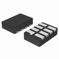
IC XLATOR 2BIT NONINV DUAL 8UDFN

NLSV2T244MUTAG

Manufacturer Part Number
NLSV2T244MUTAG
Description
IC XLATOR 2BIT NONINV DUAL 8UDFN
Manufacturer
ON Semiconductor
Datasheet

Specifications of NLSV2T244MUTAG

Logic Function
Translator, 3-State
Number Of Bits
2
Input Type
Voltage
Output Type
Voltage
Number Of Channels
2
Number Of Outputs/channel
2
Differential - Input:output
No/No
Propagation Delay (max)
1.6ns
Voltage - Supply
0.9 V ~ 4.5 V
Operating Temperature
-40°C ~ 85°C
Package / Case
8-UFDFN
Supply Voltage
3 V ~ 3.6 V
High Level Output Current
-24mA
Low Level Output Current
24mA
Operating Supply Voltage (typ)
1.8/2.5/3.3V
Package Type
uDFN
Operating Supply Voltage (max)
4.5V
Operating Supply Voltage (min)
0.9V
Abs. Propagation Delay Time
5.3ns
Mounting
Surface Mount
Pin Count
8
Operating Temperature (min)
-40C
Operating Temperature (max)
85C
Operating Temperature Classification
Industrial
Lead Free Status / RoHS Status
Lead free / RoHS Compliant
Data Rate
-
Lead Free Status / Rohs Status
Compliant

Available stocks

Company
Part Number
Manufacturer
Quantity
Price
Part Number:
NLSV2T244MUTAG
Manufacturer:
ONSemicon
Quantity:
43 649
Part Number:
NLSV2T244MUTAG
Manufacturer:
ON/安森美
Quantity:
20 000
Company:
Part Number:
NLSV2T244MUTAG
Quantity:
744 000
NLSV2T244
2-Bit Dual-Supply
Non-Inverting Level
Translator
translator. The input A
different power supply rails, V
supply rails are configurable from 0.9 V to 4.5 V allowing universal
low−voltage translation from the input A
Features
Typical Applications
Important Information
© Semiconductor Components Industries, LLC, 2009
December, 2009 − Rev. 1
The NLSV2T244 is a 2−bit configurable dual−supply voltage level
Wide V
High−Speed w/ Balanced Propagation Delay
Inputs and Outputs have OVT Protection to 4.5 V
Non−preferential V
Outputs at 3−State until Active V
Power−Off Protection
Outputs Switch to 3−State with V
Small Packaging: UDFN8, SO−8, Micro8
This is a Pb−Free Device
Mobile Phones, PDAs, Other Portable Devices
ESD Protection for All Pins:
CCA
HBM (Human Body Model) > 5000 V
and V
CCB
CCA
n
and output B
Operating Range: 0.9 V to 4.5 V
and V
CCB
CCA
CC
CCB
n
Sequencing
ports are designed to track two
and V
is Reached
n
at GND
to the output B
CCB
respectively. Both
n
port.
1
†For information on tape and reel specifications,
NLSV2T244MUTAG
NLSV2T244DR2G
NLSV2T244DMR2G
8
including part orientation and tape sizes, please
refer to our Tape and Reel Packaging Specification
Brochure, BRD8011/D.
1
1
1
Device
A
Y
W
G
8
ORDERING INFORMATION
A
L
Y
W
G
UP = Specific Device Code
M
G
= Pb−Free Package
http://onsemi.com
= Pb−Free Package
= Date Code
= Pb−Free Package
CASE 517AJ
MU SUFFIX
DM SUFFIX
CASE 846A
= Assembly Location
= Year
= Work Week
CASE 751
UDFN8
D SUFFIX
= Assembly Location
= Wafer Lot
= Year
= Work Week
Micro8
SO−8
(Pb−Free)
(Pb−Free)
(Pb−Free)
Package
UDFN8
Micro8
SO−8
Publication Order Number:
3000/Tape & Reel
2500/Tape & Reel
4000/Tape & Reel
DIAGRAMS
8
1
MARKING
NLSV2T244/D
Shipping
8
1
AYW G
ALYW G
UPM
2T244
244
G
G
G

Related parts for NLSV2T244MUTAG

NLSV2T244MUTAG Summary of contents

Page 1

... HBM (Human Body Model) > 5000 V © Semiconductor Components Industries, LLC, 2009 December, 2009 − Rev. 1 ports are designed to track two and V respectively. Both CCB to the output B port Reached at GND NLSV2T244MUTAG NLSV2T244DR2G NLSV2T244DMR2G †For information on tape and reel specifications, 1 http://onsemi.com MARKING DIAGRAMS UDFN8 8 UPM MU SUFFIX G ...

Page 2

CCA CCB GND UDFN8 (Top View) PIN ASSIGNMENT PIN FUNCTION V Input Port DC Power Supply CCA V Output Port DC Power ...

Page 3

MAXIMUM RATINGS Symbol Rating Supply Voltage CCA CCB V DC Input Voltage I V Control Input Output Voltage Input Diode Current Output Diode Current ...

Page 4

DC ELECTRICAL CHARACTERISTICS Symbol Parameter V Input HIGH Voltage IH (An, OE) V Input LOW Voltage IL (An, OE) V Output HIGH Voltage OH V Output LOW Voltage OL I Input Leakage Current I I Power−Off Leakage Current OFF I ...

Page 5

TOTAL STATIC POWER CONSUMPTION (I 4.5 V (V) Min Max CCA 4.5 2 3.3 2 2.8 < 2 1.8 < 1 0.9 < 0.5 NOTE: Connect ground before applying supply voltage and V will not damage the ...

Page 6

Pulse Generator Figure 2. AC (Propagation Delay) Test Circuit Test PLH PHL PLZ PZL PHZ PZH equivalent (includes probe and jig capacitance ...

Page 7

0.10 C PIN ONE E REFERENCE É É É É 0.10 C TOP VIEW (A3 SIDE VIEW e/2 DETAIL (b2 (L2 ...

Page 8

... G C SEATING PLANE −Z− 0.25 (0.010 *For additional information on our Pb−Free strategy and soldering details, please download the ON Semiconductor Soldering and Mounting Techniques Reference Manual, SOLDERRM/D. PACKAGE DIMENSIONS SO−8 CASE 751−07 ISSUE 0.10 (0.004 SOLDERING FOOTPRINT* 1 ...

Page 9

... A1 *For additional information on our Pb−Free strategy and soldering details, please download the ON Semiconductor Soldering and Mounting Techniques Reference Manual, SOLDERRM/D. ON Semiconductor and are registered trademarks of Semiconductor Components Industries, LLC (SCILLC). SCILLC reserves the right to make changes without further notice to any products herein ...

Related keywords