AT93C46D-PU Atmel, AT93C46D-PU Datasheet
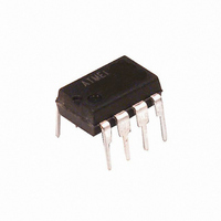
IC EEPROM 1KBIT 2MHZ 8DIP

AT93C46D-PU

Manufacturer Part Number
AT93C46D-PU
Description
IC EEPROM 1KBIT 2MHZ 8DIP
Manufacturer
Atmel
Datasheets

Specifications of AT93C46D-PU

Format - Memory
EEPROMs - Serial
Memory Type
EEPROM
Memory Size
1K (128 x 8 or 64 x 16)
Speed
250kHz, 1MHz, 2MHz
Interface
3-Wire Serial
Voltage - Supply
1.8 V ~ 5.5 V
Operating Temperature
-40°C ~ 85°C
Package / Case
8-DIP (0.300", 7.62mm)
Organization
128 K x 8 or 64 K x 16
Interface Type
3-Wire
Maximum Clock Frequency
2 MHz
Supply Voltage (max)
5.5 V
Supply Voltage (min)
1.8 V
Maximum Operating Current
2 mA
Maximum Operating Temperature
+ 85 C
Mounting Style
Through Hole
Minimum Operating Temperature
- 40 C
Operating Supply Voltage
1.8 V, 5.5 V
Capacitance, Input
5 pF
Capacitance, Output
5 pF
Current, Input, Leakage
0.1 μA
Current, Operating
2 mA
Current, Output, Leakage
0.1
Data Retention
100 yrs.
Density
1K
Package Type
PDIP
Temperature, Operating
-40 to +85 °C
Time, Address Setup
200
Time, Fall
1000 ns
Time, Rise
1000 ns
Voltage, Input, High
2.8 to 6.5 V
Voltage, Input, Low
0.54 to 1.65 V
Voltage, Output, High
1.6 V
Voltage, Output, Low
0.2 V
Voltage, Supply
1.8 to 5.5 V
Memory Configuration
128 X 8, 64 X 16
Clock Frequency
2MHz
Supply Voltage Range
1.8V To 5.5V
Memory Case Style
DIP
No. Of Pins
8
Rohs Compliant
Yes
Lead Free Status / RoHS Status
Lead free / RoHS Compliant

Available stocks

Company
Part Number
Manufacturer
Quantity
Price
Part Number:
AT93C46D-PU
Manufacturer:
ATMEL
Quantity:
500
Part Number:
AT93C46D-PU
Manufacturer:
ATMEL
Quantity:
4 500
Part Number:
AT93C46D-PU
Manufacturer:
ATMEL
Quantity:
20 000
Features
Description
The AT93C46D provides 1024 bits of serial electrically erasable programmable read-
only memory (EEPROM), organized as 64 words of 16 bits each (when the ORG pin is
connected to VCC), and 128 words of 8 bits each (when the ORG pin is tied to
ground). The device is optimized for use in many industrial and commercial applica-
tions where low-power and low-voltage operations are essential. The AT93C46D is
available in space-saving 8-lead PDIP, 8-lead JEDEC SOIC, 8-lead Ultra Thin mini-
MAP (MLP 2x3), 8-lead TSSOP, and 8-lead dBGA2 packages.
The AT93C46D is enabled through the Chip Select pin (CS) and accessed via a
three-wire serial interface consisting of Data Input (DI), Data Output (DO), and Shift
Clock (SK). Upon receiving a Read instruction at DI, the address is decoded and the
data is clocked out serially on the DO pin. The Write cycle is completely self-timed,
and no separate Erase cycle is required before Write. The Write cycle is only enabled
when the part is in the Erase/Write Enable state. When CS is brought high following
the initiation of a Write cycle, the DO pin outputs the Ready/Busy status of the part.
The AT93C46D is available in 1.8 (1.8V to 5.5V) version.
Table 0-1.
Pin Name
CS
SK
DI
DO
GND
VCC
ORG
NC
Low-voltage and Standard-voltage Operation
User-selectable Internal Organization
Three-wire Serial Interface
2 MHz Clock Rate (5V)
Self-timed Write Cycle (5 ms max)
High Reliability
8-lead JEDEC PDIP, 8-lead JEDEC SOIC, 8-lead Ultra Thin mini-MAP (MLP 2x3), 8-lead
TSSOP and 8-ball dBGA2 Packages
Die Sales: Wafer Form, Tape and Reel, and Bumped Wafers
– 1.8 (V
– 1K: 128 x 8 or 64 x 16
– Endurance: 1 Million Write Cycles
– Data Retention: 100 Years
CC
= 1.8V to 5.5V)
Pin Configurations
Function
Chip Select
Serial Data Clock
Serial Data Input
Serial Data Output
Ground
Power Supply
Internal Organization
No Connect
DO
CS
SK
DI
DO
CS
SK
DI
1
2
3
4
8-lead SOIC
8-lead PDIP
1
2
3
4
DO
CS
SK
DI
8
7
6
5
8
7
6
5
VCC
NC
ORG
GND
8-lead TSSOP
1
2
3
4
VCC
NC
ORG
GND
8-lead Ultra Thin mini-MAP (MLP 2x3)
8
7
6
5
ORG
GND
ORG
VCC
GND
VCC
NC
NC
8-lead dBGA2
VCC
NC
ORG
GND
Bottom View
Bottom View
8
7
6
5
8
7
6
5
1
2
3
4
CS
SK
D1
D0
1
2
3
4
CS
SK
DI
DO
Three-wire
Serial
EEPROM
1K (128 x 8 or 64 x 16)
AT93C46D

Related parts for AT93C46D-PU

AT93C46D-PU Summary of contents

Page 1

... PDIP, 8-lead JEDEC SOIC, 8-lead Ultra Thin mini- MAP (MLP 2x3), 8-lead TSSOP, and 8-lead dBGA2 packages. The AT93C46D is enabled through the Chip Select pin (CS) and accessed via a three-wire serial interface consisting of Data Input (DI), Data Output (DO), and Shift Clock (SK) ...

Page 2

... If the ORG pin is left unconnected and the application does not load the input beyond the capability of the internal 1 Meg ohm pullup, then the “x 16” organization is selected. 2. For the AT93C46D, if the “x 16” organization is the mode of choice and pin 6 (ORG) is left ® unconnected, Atmel recommends using AT93C46E device ...

Page 3

... 2 2.7V ≤ V ≤ 5.5V CC − 0 0. 1.8V ≤ V ≤ 2.7V CC − 100 µA OH AT93C46D = +1.8V (unless otherwise noted) CC Max Units +1.8V to +5.5V (unless otherwise noted) CC Min Typ Max 1.8 5.5 2.7 5.5 4.5 5.5 0.5 2.0 0.5 2.0 0.4 1 ...

Page 4

... Output Delay to “0” PD0 Status Valid High t DF Impedance t Write Cycle Time WP (1) Endurance 5.0V, 25°C Note: 1. This parameter is ensured by characterization. AT93C46D 4 = −40° 85° Test Condition 4.5V ≤ V ≤ 5.5V CC 2.7V ≤ V ≤ 5.5V CC 1.8V ≤ V ≤ 5.5V CC 4.5V ≤ V ≤ 5.5V CC 2.7V ≤ ...

Page 5

... AT93C46D Ordering Information Ordering Code AT93C46D-PU (Bulk form only) (1) AT93C46DN-SH-B (NiPdAu Lead finish) (2) AT93C46DN-SH-T (NiPdAu Lead finish) (1) AT93C46D-TH-B (NiPdAu Lead finish) (2) AT93C46D-TH-T (NiPdAu Lead finish) (2) AT93C46DY6-YH-T (NiPdAu Lead finish) (2) AT93C46DU3-UU-T (3) AT93C46D-W-11 Notes: 1. “-B” denotes bulk 2. “-T” denotes tape and reel. SOIC = 4K per reel. TSSOP, Ultra Thin Mini MAP, and dBGA2 = 5K per reel. ...

Page 6

... Dambar protrusions. Dambar protrusions shall not exceed 0.010 (0.25 mm). 2325 Orchard Parkway San Jose, CA 95131 TITLE 8P3, 8-lead, 0.300" Wide Body, Plastic Dual In-line Package (PDIP) AT93C46D End View COMMON DIMENSIONS (Unit of Measure = inches) MIN NOM MAX SYMBOL A 0.210 A2 0.115 ...

Related keywords