AT24C16BN-SH-B Atmel, AT24C16BN-SH-B Datasheet
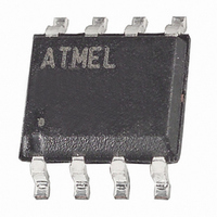
IC EEPROM 16KBIT 1MHZ 8SOIC

AT24C16BN-SH-B

Manufacturer Part Number
AT24C16BN-SH-B
Description
IC EEPROM 16KBIT 1MHZ 8SOIC
Manufacturer
Atmel
Datasheets

Specifications of AT24C16BN-SH-B

Format - Memory
EEPROMs - Serial
Memory Type
EEPROM
Memory Size
16K (2K x 8)
Speed
400kHz, 1MHz
Interface
I²C, 2-Wire Serial
Voltage - Supply
1.8 V ~ 5.5 V
Operating Temperature
-40°C ~ 85°C
Package / Case
8-SOIC (3.9mm Width)
Organization
256 K x 8
Interface Type
2-Wire
Maximum Clock Frequency
1 MHz
Supply Voltage (max)
3.6 V
Supply Voltage (min)
1.8 V
Maximum Operating Current
3 mA
Maximum Operating Temperature
+ 85 C
Mounting Style
SMD/SMT
Minimum Operating Temperature
- 40 C
Operating Supply Voltage
1.8 V, 3.6 V
Capacitance, Input
6 pF
Capacitance, Output
8 pF
Current, Input, Leakage
0.1 μA
Current, Operating
1 mA (Read), 2 mA (Write)
Current, Output, Leakage
0.05
Data Retention
100 yrs.
Density
16K
Package Type
JEDEC SOIC
Temperature, Operating
-40 to +85 °C
Time, Access
0.55 μs
Time, Fall
300 ns
Time, Rise
0.3 μs
Voltage, Input, High
2.3 to 6 V
Voltage, Input, Low
0.54 to 1.65 V
Voltage, Output, Low
0.2 V
Voltage, Supply
1.8 to 5.5 V
Lead Free Status / RoHS Status
Lead free / RoHS Compliant

Available stocks

Company
Part Number
Manufacturer
Quantity
Price
Part Number:
AT24C16BN-SH-B
Manufacturer:
ATMEL/爱特梅尔
Quantity:
20 000
1. Features
2. Description
The AT24C16B provides 16384 bits of serial electrically erasable and programmable
read-only memory (EEPROM) organized as 2048 words of 8 bits each. The device is
optimized for use in many industrial and commercial applications where low-power
and low-voltage operation are essential. The AT24C16B is available in space-saving
8-lead PDIP, 8-lead JEDEC SOIC, 8-lead Ultra Thin Mini-MAP (MLP 2x3)
SOT23, 8-lead Ultra Lead Frame Land Grid Array (ULA), 8-lead TSSOP, and 8-ball
dBGA2 packages and is accessed via a Two-wire serial interface. In addition, the
AT24C16B is available in 1.8V (1.8V to 5.5V) version.
Table 2-1.
Pin Name
NC
SDA
SCL
WP
GND
VCC
Low-voltage and Standard-voltage Operation
Internally Organized 2048 x 8 (16K)
Two-wire Serial Interface
Schmitt Trigger, Filtered Inputs for Noise Suppression
Bidirectional Data Transfer Protocol
1 MHz (5V, 2.5V), 400 kHz (1.8V) Compatibility
Write Protect Pin for Hardware Data Protection
16-byte Page (16K) Write Modes
Partial Page Writes Allowed
Self-timed Write Cycle (5 ms max)
High-reliability
8-lead PDIP, 8-lead JEDEC SOIC, 8-lead Ultra-Thin Mini-MAP (MLP 2x3), 5-lead SOT23,
8-lead Ultra Lead Frame Land Grid Array (ULA), 8-lead TSSOP and 8-ball dBGA2
Packages
Lead-free/Halogen-free
Die Sales: Wafer Form, Tape and Reel, and Bumped Wafers
8-lead Ultra Lead Frame
– 1.8 (V
– Endurance: 1 Million Write Cycles
– Data Retention: 100 Years
Land Grid Array (ULA)
VCC
SDA
SCL
WP
Bottom View
CC
8
7
6
5
No Connect
Serial Data
Serial Clock Input
Write Protect
Ground
Function
Power Supply
= 1.8V to 5.5V)
Pin Configuration
1
2
3
4
NC
NC
NC
GND
GND
SDA
SCL
Mini-MAP (MLP 2x3)
GND
VCC
NC
NC
NC
SDA
8-lead Ultra Thin
SCL
WP
8-lead TSSOP
5-lead SOT23
Bottom View
1
2
3
8
7
6
5
1
2
3
4
1
2
3
4
8
7
6
5
5
4
NC
NC
NC
GND
VCC
WP
SCL
SDA
WP
VCC
GND
NC
NC
NC
GND
VCC
SDA
NC
NC
NC
SCL
WP
8-ball dBGA2
Bottom View
8-lead SOIC
8-lead PDIP
1
2
3
4
8
7
6
5
1
2
3
4
1
2
3
4
8
7
6
5
8
7
6
5
NC
NC
NC
GND
,
VCC
WP
SCL
SDA
5-lead
VCC
WP
SCL
SDA
Two-wire
Serial EEPROM
16K (2048 x 8)
AT24C16B

Related parts for AT24C16BN-SH-B

AT24C16BN-SH-B Summary of contents

Page 1

... Description The AT24C16B provides 16384 bits of serial electrically erasable and programmable read-only memory (EEPROM) organized as 2048 words of 8 bits each. The device is optimized for use in many industrial and commercial applications where low-power and low-voltage operation are essential. The AT24C16B is available in space-saving ...

Page 2

Absolute Maximum Ratings Operating Temperature..................................–55°C to +125°C Storage Temperature .....................................–65°C to +150°C Voltage on Any Pin with Respect to Ground .................................... –1.0V to +7.0V Maximum Operating Voltage .......................................... 6.25V DC Output Current........................................................ 5.0 mA Figure 2-1. Block Diagram VCC GND ...

Page 3

Table 4-1. Pin Capacitance Applicable over recommended operating range from T Symbol Test Condition C Input/Output Capacitance (SDA) I/O C Input Capacitance (SCL) IN Note: 1. This parameter is characterized and is not 100% tested. Table 4-2. DC Characteristics ...

Page 4

Table 4-3. AC Characteristics (Industrial Temperature) Applicable over recommended operating range from T erwise noted). Test conditions are listed in Note 2. Symbol Parameter f Clock Frequency, SCL SCL t Clock Pulse Width Low LOW t Clock Pulse Width High ...

Page 5

... AT24C16B Ordering Information Ordering Codes AT24C16B-PU (Bulk Form Only) (1) AT24C16BN-SH-B (NiPdAu Lead Finish) (2) AT24C16BN-SH-T (NiPdAu Lead Finish) (1) AT24C16B-TH-B (NiPdAu Lead Finish) (2) AT24C16B-TH-T (NiPdAu Lead Finish) (2) AT24C16BY6-YH-T (NiPdAu Lead Finish) (2) AT24C16BD3-DH-T (NiPdAu Lead Finish) (2) AT24C16BTSU-T (2) AT24C16BU3-UU-T (3) AT24C16B-W-11 Notes: 1. “-B” denotes bulk. ...

Page 6

JEDEC SOIC Top View e Side View Note: These drawings are for general information only. Refer to JEDEC Drawing MS-012, Variation AA for proper dimensions, tolerances, datums, etc. 1150 E. Cheyenne Mtn. Blvd. Colorado Springs, CO 80906 ...

Related keywords