CY7C1041DV33-10ZSXI Cypress Semiconductor Corp, CY7C1041DV33-10ZSXI Datasheet
CY7C1041DV33-10ZSXI
Specifications of CY7C1041DV33-10ZSXI
CY7C1041DV33-10ZSXI
Available stocks


Related parts for CY7C1041DV33-10ZSXI


CY7C1041DV33-10ZSXI Summary of contents
Page 1
... Document Number: 38-05473 Rev. *I 4-Mbit (256 K × 16) Static RAM Functional Description The CY7C1041DV33 is a high performance CMOS Static RAM organized as 256 K words by 16-bits. To write to the device, take chip enable (CE) and write enable (WE) inputs LOW. If byte low enable (BLE) is LOW, then data from I/O pins (I/O ...
Page 2
... Thermal Resistance .......................................................... 5 AC Test Loads and Waveforms ....................................... 5 AC Switching Characteristics ......................................... 6 Data Retention Characteristics ....................................... 7 Data Retention Waveform ................................................ 7 Switching Waveforms ...................................................... 7 Truth Table ...................................................................... 10 Document Number: 38-05473 Rev. *I CY7C1041DV33 Ordering Information ...................................................... 11 Ordering Code Definitions ......................................... 11 Package Diagrams .......................................................... 12 Acronyms ........................................................................ 15 Document Conventions ................................................. 15 Units of Measure ....................................................... 15 Document History Page ................................................. 16 Sales, Solutions, and Legal Information ...................... 17 Worldwide Sales and Design Support ...
Page 3
... Pinout 1 is compliant with CY7C1041CV33 and pinout 2 is JEDEC compliant. The difference between the two is that the higher and lower byte I/Os (I/O balls) are swapped. Document Number: 38-05473 Rev. *I –10 (Automotive- [3, 4] Figure 2. 48-ball VFBGA (Pinout BLE Figure 3. 44-pin SOJ/TSOP BHE BLE CY7C1041DV33 [2] [2] –12 (Automotive-E) Unit [ BHE [7:0] Page and I/O [15:8] [+] Feedback ...
Page 4
... MAX , – – 0 – 0 < 0 for pulse durations of less than 20 ns. CY7C1041DV33 Ambient V Speed CC Temperature –40 °C to +85 °C 3.3 V ± 0.3 V [1] –40 °C to +85 °C 3.3 V ± 0.3 V [1] –40 °C to +125 °C 3.3 V ± 0.3 V –10 –12 [6] [6] ...
Page 5
... A CC Test Conditions Still Air, soldered × 4.5 inch, four layer printed circuit board [8] 3.0V 50 Ω 30 pF* GND 1.5V Rise Time: 1 V/ns (a) R2 351Ω AC Test Loads and Waveforms CY7C1041DV33 Max Unit FBGA SOJ TSOP II Package Package Package 27.89 57.91 50.66 14 ...
Page 6
... CC AC Test Loads and is less than less than HZCE LZCE HZOE LZOE HZBE and t HZWE CY7C1041DV33 –10 –12 [10] [10] (Automotive-E) Max Min Max – 100 – 10 – 12 – – 10 – – ...
Page 7
... < 0 DATA RETENTION MODE 3 > CDR [20, 21] Figure 4. Read Cycle No OHA > 50 μs or stable at V > 50 μ CC(min.) CC(min CY7C1041DV33 [16] Min Max 2.0 – – 0.3 V, Industrial – 10 [17] Auto-A – 10 [17] Auto-E – – t – DATA VALID Page ...
Page 8
... Data I/O is high impedance BHE and BLE = V 25 goes HIGH simultaneously with WE going HIGH, the output remains in a high impedance state. Document Number: 38-05473 Rev DOE t LZOE DBE LZBE DATA VALID 50 SCE PWE t BW IH. CY7C1041DV33 [22, 23] t HZOE t HZCE t HZBE HIGH IMPEDANCE 50% I [24, 25 Page ICC ...
Page 9
... If CE goes HIGH simultaneously with WE going HIGH, the output remains in a high impedance state. 28. During this period the I/Os are in the output state and input signals should not be applied. Document Number: 38-05473 Rev PWE t SCE SCE PWE t SD DATA VALID IN IH. CY7C1041DV33 [26, 27 Page [+] Feedback ...
Page 10
... Power-down Data out Read all bits High Z Read lower bits only Data out Read upper bits only Data in Write all bits High Z Write lower bits only Data in Write upper bits only High Z Selected, outputs disabled CY7C1041DV33 LZWE Mode Power Standby ( Active ( ...
Page 11
... Ordering Information Speed (ns) Ordering Code 10 CY7C1041DV33-10BVI CY7C1041DV33-10BVXI CY7C1041DV33-10BVJXI CY7C1041DV33-10VXI CY7C1041DV33-10ZSXI 10 CY7C1041DV33-10BVXA CY7C1041DV33-10ZSXA 12 CY7C1041DV33-12BVXE CY7C1041DV33-12BVJXE CY7C1041DV33-12VXE CY7C1041DV33-12ZSXE Please contact your local Cypress sales representative for availability of these parts Ordering Code Definitions V33 - xx xxx Document Number: 38-05473 Rev. *I Package Diagram Package Type 51-85150 ...
Page 12
... Package Diagrams Figure 1. 48-ball VFBGA (6 × 8 × 1 mm), 51-85150 a Document Number: 38-05473 Rev. *I CY7C1041DV33 51-85150 *F Page [+] Feedback ...
Page 13
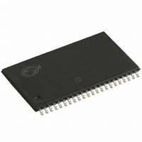
... Package Diagrams (continued) Figure 2. 44-pin (400-mil) Molded SOJ, 51-85082 Document Number: 38-05473 Rev. *I CY7C1041DV33 51-85082 *C Page [+] Feedback ...
Page 14
... Package Diagrams (continued) Document Number: 38-05473 Rev. *I Figure 3. 44-pin TSOP II, 51-85087 CY7C1041DV33 51-85087 *C Page [+] Feedback ...
Page 15
... Input/output OE output enable SRAM Static random access memory SOJ Small Outline J-Lead TSOP Thin Small Outline Package VFBGA Very Fine-Pitch Ball Grid Array Document Number: 38-05473 Rev. *I CY7C1041DV33 Document Conventions Units of Measure Symbol Unit of Measure ns nano seconds V Volts µA micro Amperes mA ...
Page 16
... Document History Page Document Title: CY7C1041DV33 4-Mbit (256 K × 16) Static RAM Document Number: 38-05473 Orig. of Submission Rev. ECN No. Change ** 201560 SWI See ECN *A 233729 RKF See ECN *B 351117 PCI See ECN *C 446328 NXR See ECN *D 480177 VKN See ECN *E 2541850 VKN/PYRS ...
Page 17
... Cypress against all charges. Use may be limited by and subject to the applicable Cypress software license agreement. Document Number: 38-05473 Rev. *I All products and company names mentioned in this document may be the trademarks of their respective holders. cypress.com/go/plc Revised January 24, 2011 CY7C1041DV33 PSoC Solutions psoc.cypress.com/solutions PSoC 1 | PSoC 3 ...