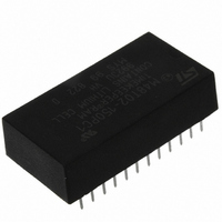
M48Z02-150PC1 STMicroelectronics, M48Z02-150PC1 Datasheet

M48Z02-150PC1
Specifications of M48Z02-150PC1
Available stocks
Related parts for M48Z02-150PC1
M48Z02-150PC1 Summary of contents
Page 1
... READ cycle time equals WRITE cycle time ■ Automatic power-fail chip deselect and WRITE protection ■ WRITE protect voltages (V = Power-fail deselect voltage): PFD – M48Z02 4. 4.5 V ≤ V ≤ 4.75 V PFD – M48Z12 4 4.2 V ≤ V ≤ 4.5 V PFD ■ ...
Page 2
... The M48Z02/ non-volatile pin and function equivalent to any JEDEC standard SRAM. It also easily fits into many ROM, EPROM, and EEPROM sockets, providing the non-volatility of PROMs without any requirement for special WRITE timing or limitations on the number of WRITEs that can be performed ...
Page 3
... Write mode The M48Z02/ the WRITE mode whenever W and E are active. The start of a WRITE is referenced from the latter occurring falling edge WRITE is terminated by the earlier rising edge The addresses must be held valid throughout the cycle must return high for a minimum the initiation of another READ or WRITE cycle ...
Page 4
... For more information on a battery storage life refer to the application note AN1012. 10/21 (1) Min 70°C or –40 to 85° falls within the V CC PFD . The M48Z02/12 may respond to transient noise spikes rises, the battery voltage is checked. If the voltage is too SO CC M48Z02, M48Z12 M48Z02/M48Z12 –70 –150 –200 Max Min Max Min 150 200 120 90 ...
Page 5
... M48Z02, M48Z12 3 Maximum ratings Stressing the device above the rating listed in the absolute maximum ratings table may cause permanent damage to the device. These are stress ratings only and operation of the device at these or any other conditions above those indicated in the operating sections of this specification is not implied ...
Page 6
... At 25° MHz. 3. Outputs deselected. 14/21 conditions. Designers should check that the operating Parameter ) ) Grade DEVICE UNDER TEST 1kΩ includes JIG capacitance (1)(2) Parameter M48Z02, M48Z12 M48Z02 M48Z12 4.75 to 5.5 4 100 100 ≤ 5 ≤ 1.5 1.5 5V 1.8kΩ OUT ...
Page 7
... M48Z02, M48Z12 Table 8. DC characteristics Symbol Parameter I Input leakage current LI (2) I Output leakage current LO I Supply current CC I Supply current (standby) TTL CC1 I Supply current (standby) CMOS CC2 V Input low voltage IL V Input high voltage IH V Output low voltage OL V Output high voltage OH 1 ...
Page 8
... V (min). CC PFD fall time of less than t may cause corruption of RAM data. FB (1)(2) Parameter M48Z02 M48Z12 . 70° M48Z02, M48Z12 Min Max 0 300 4. 4.5 to 5.5 V (except where CC Min Typ Max 4.5 4.6 4 ...
Page 9
... M48Z02, M48Z12 5 Package mechanical data In order to meet environmental requirements, ST offers these devices in ECOPACK packages. These packages have a lead-free second level interconnect. The category of second Level Interconnect is marked on the package and on the inner box label, in compliance with JEDEC Standard JESD97. The maximum ratings related to soldering conditions are also marked on the inner box label ...
Page 10
... V = 4. 4 Speed – (M48Z02/12) –150 = 150 ns (M48Z02/12) –200 = 200 ns (M48Z02/12) Package PC = PCDIP24 Temperature range 70°C Shipping method ® blank = ECOPACK For a list of available options (e.g., speed, package) or for further information on any aspect of this device, please contact the ST sales office nearest you. ...


