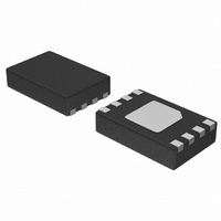
CAT34C02VP2I-GT4 ON Semiconductor, CAT34C02VP2I-GT4 Datasheet - Page 4

CAT34C02VP2I-GT4
Manufacturer Part Number
CAT34C02VP2I-GT4
Description
IC EEPROM 2KBIT 400KHZ 8TDFN
Manufacturer
ON Semiconductor
Specifications of CAT34C02VP2I-GT4
Format - Memory
EEPROMs - Serial
Memory Type
EEPROM
Memory Size
2K (256 x 8)
Speed
400kHz
Interface
I²C, 2-Wire Serial
Voltage - Supply
1.7 V ~ 5.5 V
Operating Temperature
-40°C ~ 85°C
Package / Case
8-VFDFN Exposed Pad
Density
2Kb
Interface Type
Serial (I2C)
Organization
256x8
Access Time (max)
900ns
Frequency (max)
400KHz
Write Protection
Yes
Data Retention
100Year
Operating Supply Voltage (typ)
1.8/2.5/3.3/5V
Operating Temp Range
-40C to 85C
Supply Current
2mA
Operating Supply Voltage (min)
1.7V
Operating Supply Voltage (max)
5.5V
Operating Temperature Classification
Industrial
Mounting
Surface Mount
Pin Count
8
Lead Free Status / RoHS Status
Lead free / RoHS Compliant
Other names
34C02VP2I-GT4
CAT34C02VP2I-GT4TR
CAT34C02VP2I-GT4TR
Available stocks
Company
Part Number
Manufacturer
Quantity
Price
Company:
Part Number:
CAT34C02VP2I-GT4
Manufacturer:
ON Semiconductor
Quantity:
83 445
Company:
Part Number:
CAT34C02VP2I-GT4
Manufacturer:
ON Semiconductor
Quantity:
3 000
Part Number:
CAT34C02VP2I-GT4
Manufacturer:
ON/安森美
Quantity:
20 000
Power−On Reset (POR)
circuitry which protects the internal logic against powering
up in the wrong state.
V
Reset mode when V
This bi−directional POR feature protects the device against
‘brown−out’ failure following a temporary loss of power.
Pin Description
SCL: The Serial Clock input pin accepts the Serial Clock
generated by the Master.
SDA: The Serial Data I/O pin receives input data and
transmits data stored in EEPROM. In transmit mode, this pin
is open drain. Data is acquired on the positive edge, and is
delivered on the negative edge of SCL.
A
These pins have on−chip pull−down resistors.
WP: The Write Protect input pin inhibits all write
operations, when pulled HIGH. This pin has an on−chip
pull−down resistor.
Functional Description
(I
that sends data to the bus as a transmitter and a device
receiving data as a receiver. Data flow is controlled by a
Master device, which generates the serial clock and all
START and STOP conditions. The CAT34C02 acts as a
Slave device. Master and Slave alternate as either
transmitter or receiver. Up to 8 devices may be connected to
the bus as determined by the device address inputs A
and A
I
two wires are connected to the V
resistors. Master and Slave devices connect to the 2−wire
bus via their respective SCL and SDA pins. The transmitting
2
CC
0
2
C Bus Protocol
The CAT34C02 incorporates Power−On Reset (POR)
The CAT34C02 will power up into Standby mode after
The CAT34C02 supports the Inter−Integrated Circuit
The I
C) Bus data transmission protocol, which defines a device
, A
exceeds the POR trigger level and will power down into
1
2
.
and A
2
C bus consists of two ‘wires’, SCL and SDA. The
2
: The Address pins accept the device address.
CC
SDA
SCL
drops below the POR trigger level.
START BIT
CC
supply via pull−up
Figure 2. Start/Stop Timing
http://onsemi.com
0
, A
1
,
4
device pulls down the SDA line to ‘transmit’ a ‘0’ and
releases it to ‘transmit’ a ‘1’.
busy (see A.C. Characteristics).
while the SCL line is HIGH. An SDA transition while SCL
is HIGH will be interpreted as a START or STOP condition
(Figure 2).
Start
of a HIGH to LOW transition on SDA while SCL is HIGH.
The START acts as a ‘wake−up’ call to all receivers. Absent
a START, a Slave will not respond to commands.
Stop
of a LOW to HIGH transition on SDA while SCL is HIGH.
The STOP starts the internal Write cycle (when following a
Write command) or sends the Slave into standby mode
(when following a Read command).
Device Addressing
condition on the bus. The Master then broadcasts an 8−bit
serial Slave address. The first 4 bits of the Slave address are
set to 1010, for normal Read/Write operations (Figure 3).
The next 3 bits, A
devices. The last bit, R/W, specifies whether a Read (1) or
Write (0) operation is to be performed.
Acknowledge
with an acknowledge (ACK) by pulling down the SDA line
during the 9
acknowledge the byte address and every data byte presented
in Write mode. In Read mode the Slave shifts out a data byte,
and then releases the SDA line during the 9
the Master acknowledges the data, then the Slave continues
transmitting. The Master terminates the session by not
acknowledging the last data byte (NoACK) and by sending
a STOP to the Slave. Bus timing is illustrated in Figure 5.
Data transfer may be initiated only when the bus is not
During data transfer, the SDA line must remain stable
The START condition precedes all commands. It consists
The STOP condition completes all commands. It consists
The Master initiates data transfer by creating a START
After processing the Slave address, the Slave responds
th
clock cycle (Figure 4). The Slave will also
2
, A
STOP BIT
1
and A
0
, select one of 8 possible Slave
th
clock cycle. If


