HYB25D512160CE-5 Qimonda, HYB25D512160CE-5 Datasheet - Page 33
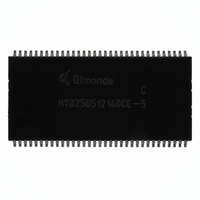
HYB25D512160CE-5
Manufacturer Part Number
HYB25D512160CE-5
Description
IC DDR SDRAM 512MBIT 66TSOP
Manufacturer
Qimonda
Datasheet
1.HYB25D512800CE-6.pdf
(42 pages)
Specifications of HYB25D512160CE-5
Format - Memory
RAM
Memory Type
DDR SDRAM
Memory Size
512M (32Mx16)
Speed
200MHz
Interface
Parallel
Voltage - Supply
2.3 V ~ 2.7 V
Operating Temperature
0°C ~ 70°C
Package / Case
66-TSOP
Lead Free Status / RoHS Status
Lead free / RoHS Compliant
Other names
675-1010-2
Available stocks
Company
Part Number
Manufacturer
Quantity
Price
Company:

Part Number:
HYB25D512160CE-5
Manufacturer:
QIMONDE
Quantity:
431


Rev. 1.41, 2007-12
03292006-3TFJ-HNV3
Parameter
Operating Current: one bank; active/ precharge;
DQ, DM, and DQS inputs changing once per clock cycle; address and control inputs changing once every two
clock cycles.
Operating Current: one bank; active/read/precharge; Burst = 4;
Refer to the following page for detailed test conditions.
Precharge Power-Down Standby Current: all banks idle; power-down mode; CKE ≤
Precharge Floating Standby Current: CS ≥ V
CKE ≥
and DM.
Precharge Quiet Standby Current: CS ≥ V
control inputs stable at ≥
Active Power-Down Standby Current: one bank active; power-down mode;
CKE ≤ V
Active Standby Current: one bank active; CS ≥ V
inputs changing twice per clock cycle; address and control inputs changing once per clock cycle
Operating Current: one bank active; Burst = 2; reads; continuous burst; address and control inputs changing
once per clock cycle; 50% of data outputs changing on every clock edge; CL = 2 for DDR200 and DDR266A,
CL = 3 for DDR333;
Operating Current: one bank active; Burst = 2; writes; continuous burst; address and control inputs changing
once per clock cycle; 50% of data outputs changing on every clock edge; CL = 2 for DDR200 and DDR266A,
CL = 3 for DDR333;
Auto-Refresh Current:
Self-Refresh Current: CKE ≤ 0.2 V; external clock on;
Operating Current: four bank; four bank interleaving with BL = 4; Refer to the following page for detailed test
conditions.
V
IHMIN
ILMAX
;
;
t
CK
t
CK
=
=
t
t
CKMIN
CKMIN
t
t
CK
CK
=
=
t
, address and other control inputs changing once per clock cycle,
;
V
RC
t
t
V
IHMIN
CKMIN
CKMIN
IN
=
=
t
RFCMIN
or ≤
; I
V
REF
OUT
V
, burst refresh
for DQ, DQS and DM.
= 0 mA
ILMAX
;
V
IHMIN
IN
=
IHMIN
V
, all banks idle; CKE ≥ V
REF
IHMIN
t
RC
Date: 2007-12-13
, all banks idle;
for DQ, DQS and DM.
=
; CKE ≥
t
t
CK
RCMIN
=
33
t
;
CKMIN
V
t
CK
IHMIN
=
;
t
CKMIN
t
RC
=
IHMIN
;
t
RASMAX
;
t
CK
HY[B/I]25D512[40/80/16]0C[C/E/F/T](L)
;
=
t
CK
512-Mbit Double-Data-Rate SDRAM
t
CKMIN
V
=
ILMAX
t
CKMIN
V
, address and other
IN
;
=
t
; DQ, DM and DQS
CK
V
REF
=
t
CKMIN
for DQ, DQS
Internet Data Sheet
I
TABLE 24
DD
Conditions
Symbol
I
I
I
I
I
I
I
I
I
I
I
I
DD0
DD1
DD2P
DD2F
DD2Q
DD3P
DD3N
DD4R
DD4W
DD5
DD6
DD7
Related parts for HYB25D512160CE-5
Image
Part Number
Description
Manufacturer
Datasheet
Request
R

Part Number:
Description:
BGA
Manufacturer:
Qimonda
Datasheet:
Part Number:
Description:
BGA
Manufacturer:
Qimonda
Datasheet:
Part Number:
Description:
Manufacturer:
Qimonda
Datasheet:
Part Number:
Description:
Manufacturer:
Qimonda
Datasheet:
Part Number:
Description:
DDR2 16Mx16, 667MHz, FBGA84, leadfree
Manufacturer:
Qimonda
Datasheet:
Part Number:
Description:
DDR2 32Mx16, 533MHz, FBGA84, leadfree
Manufacturer:
Qimonda
Datasheet:

Part Number:
Description:
HYB18TC1G160BF-3.71-Gbit DDR2 SDRAM
Manufacturer:
QIMONDA Qimonda AG
Datasheet:
Part Number:
Description:
HYB18TC1G800BF-3S1-Gbit DDR2 SDRAM
Manufacturer:
QIMONDA Qimonda AG
Datasheet: