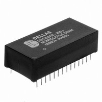
DS1244Y-70+ Maxim Integrated Products, DS1244Y-70+ Datasheet - Page 18

DS1244Y-70+
Manufacturer Part Number
DS1244Y-70+
Description
IC NVSRAM 256KBIT 70NS 28DIP
Manufacturer
Maxim Integrated Products
Datasheet
1.DS1244Y-70.pdf
(19 pages)
Specifications of DS1244Y-70+
Format - Memory
RAM
Memory Type
NVSRAM (Non-Volatile SRAM)
Memory Size
256K (32K x 8)
Speed
70ns
Interface
Parallel
Voltage - Supply
4.5 V ~ 5.5 V
Operating Temperature
0°C ~ 70°C
Package / Case
28-DIP Module (600 mil), 28-EDIP
Organization
32 K x 8
Supply Voltage (max)
5.5 V
Supply Voltage (min)
4.5 V
Operating Current
85 mA
Maximum Operating Temperature
+ 70 C
Minimum Operating Temperature
0 C
Mounting Style
SMD/SMT
Lead Free Status / RoHS Status
Lead free / RoHS Compliant
AC TEST CONDITIONS
Output Load: 50pF + 1TTL Gate
Input Pulse Levels: 0 to 3V
Timing Measurement Reference Levels
Input: 1.5V
Output: 1.5V
Input Pulse Rise and Fall Times: 5ns
NOTES:
1) WE is high for a read cycle.
2) OE = V
3) t
4) t
5) These parameters are sampled with a 50pF load and are not 100% tested.
6) If the CE low transition occurs simultaneously with or later than the WE low transition in Write
7) If the CE high transition occurs prior to or simultaneously with the WE high transition, the output
8) If WE is low or the WE low transition occurs prior to or simultaneously with the CE low transition,
9) The expected t
10) t
11) Voltages are referencd to ground.
12) RST (Pin 1) has an internal pullup resistor.
13) RTC modules can be successfully processed through conventional wave-soldering techniques as long
In addition, for the PowerCap:
1) Dallas Semiconductor recommends that PowerCap module bases experience one pass through solder
2) Hand soldering and touch-up: Do not touch or apply the soldering iron to leads for more than three
state.
going low to the earlier of CE or WE going high.
Cycle 1, the output buffers remain in a high-impedance state during this period.
buffers remain in a high-impedance state during this period.
the output buffers remain in a high-impedance state during this period.
running.
as temperature exposure to the lithium energy source contained within does not exceed +85°C. Post-
solder cleaning with water-washing techniques is acceptable, provided that ultrasonic vibration is not
used.
reflow oriented with the label side up (“live-bug”).
seconds.
– To solder, apply flux to the pad, heat the lead frame pad, and apply solder. To remove the part,
WP
DH
WR
, t
apply flux, heat the lead frame pad until the solder reflows, and use a solder wick to remove
solder.
is specified as the logical AND of CE and WE . t
is a function of the latter occurring edge of WE or CE .
DS
are measured from the earlier of CE or WE going high.
IH
or V
IL
DR
. If OE = V
is defined as cumulative time in the absence of V
IH
during write cycle, the output buffers remain in a high-impedance
18 of 19
WP
is measured from the latter of CE or WE
CC
with the clock oscillator


