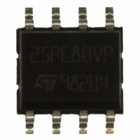
M25PE80-VMN6TP NUMONYX, M25PE80-VMN6TP Datasheet - Page 27

M25PE80-VMN6TP
Manufacturer Part Number
M25PE80-VMN6TP
Description
IC FLASH 8MBIT 75MHZ 8SOIC
Manufacturer
NUMONYX
Series
Forté™r
Datasheet
1.M25PE80-VMN6TP.pdf
(66 pages)
Specifications of M25PE80-VMN6TP
Format - Memory
FLASH
Memory Type
FLASH
Memory Size
8M (1M x 8)
Speed
75MHz
Interface
SPI, 3-Wire Serial
Voltage - Supply
2.7 V ~ 3.6 V
Operating Temperature
-40°C ~ 85°C
Package / Case
8-SOIC (3.9mm Width)
Package
8SOIC N
Cell Type
NOR
Density
8 Mb
Architecture
Sectored
Block Organization
Symmetrical
Typical Operating Supply Voltage
3.3 V
Sector Size
256Byte x 4096
Timing Type
Synchronous
Interface Type
Serial-SPI
Lead Free Status / RoHS Status
Lead free / RoHS Compliant
Other names
M25PE80-VMN6TPTR
Available stocks
Company
Part Number
Manufacturer
Quantity
Price
Company:
Part Number:
M25PE80-VMN6TP
Manufacturer:
ST
Quantity:
6 000
Part Number:
M25PE80-VMN6TP
Manufacturer:
ST
Quantity:
20 000
M25PE80
6.5
Note:
Write status register (WRSR)
The write status register (WRSR) instruction allows new values to be written to the status
register.
The status register BPi and SRWD bits are available in the M25PE80 in the T9HX process
only. See
Before the write status register (WRSR) instruction can be accepted, a write enable
(WREN) instruction must previously have been executed. After the write enable (WREN)
instruction has been decoded and executed, the device sets the write enable latch (WEL).
The write status register (WRSR) instruction is entered by driving Chip Select (S) Low,
followed by the instruction code and the data byte on serial data input (D).
The instruction sequence is shown in
The write status register (WRSR) instruction has no effect on b6, b5, b1 and b0 of the status
register. b6 and b5 are always read as 0.
Chip Select (S) must be driven High after the eighth bit of the data byte has been latched in.
If not, the write status register (WRSR) instruction is not executed. As soon as Chip Select
(S) is driven High, the self-timed write status register cycle (whose duration is t
While the write status register cycle is in progress, the status register may still be read to
check the value of the write in progress (WIP) bit. The write in progress (WIP) bit is 1 during
the self-timed write status register cycle, and is 0 when it is completed. When the cycle is
completed, the Write Enable Latch (WEL) is reset.
The write status register (WRSR) instruction allows the user to change the values of the
block protect (BP2, BP1, BP0) bits, to define the size of the area that is to be treated as
read-only, as defined in
user to set or reset the status register write disable (SRWD) bit in accordance with the Write
Protect (W) signal (see
If a write status register (WRSR) instruction is interrupted by a Reset Low pulse, the internal
cycle of the write status register operation (whose duration is t
that the supply voltage V
the reset mode (see also
Timings after a Reset Low
Figure 11. Write status register (WRSR) instruction sequence
Important note on page 6
S
C
D
Q
Table
Section
CC
Table 15: Device status after a Reset Low pulse
0
pulse).
remains within the operating range). After that the device enters
1
High Impedance
4. The write status register (WRSR) instruction also allows the
6.4.4).
2
Instruction
3
for more details.
4
Figure
5
6
11.
7
MSB
7
8
6
9 10 11 12 13 14 15
5
register in
4
Status
3
W
) is first completed (provided
2
1
0
AI02282D
and
W
Table 26:
Instructions
) is initiated.
27/66


