AT25DF021-MH-Y Atmel, AT25DF021-MH-Y Datasheet - Page 12
AT25DF021-MH-Y
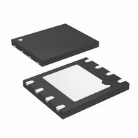
Manufacturer Part Number
AT25DF021-MH-Y
Description
IC FLASH 2MBIT 70MHZ 8UDFN
Manufacturer
Atmel
Datasheet
1.AT25DF021-SSH-B.pdf
(41 pages)
Specifications of AT25DF021-MH-Y
Format - Memory
FLASH
Memory Type
DataFLASH
Memory Size
2M (256K x 8)
Speed
70MHz
Interface
SPI, 3-Wire Serial
Voltage - Supply
2.7 V ~ 3.6 V
Operating Temperature
-40°C ~ 85°C
Package / Case
8-UDFN
Lead Free Status / RoHS Status
Lead free / RoHS Compliant


9. Protection Commands and Features
9.1
12
Write Enable
AT25DF021
While the device is executing a successful erase cycle, the Status Register can be read and will
indicate that the device is busy. For faster throughput, it is recommended that the Status Regis-
ter be polled rather than waiting the t
some point before the erase cycle completes, the WEL bit in the Status Register will be reset
back to the logical “0” state.
The device also incorporates an intelligent erase algorithm that can detect when a byte location
fails to erase properly. If an erase error occurs, it will be indicated by the EPE bit in the Status
Register.
Figure 8-4.
The Write Enable command is used to set the Write Enable Latch (WEL) bit in the Status Regis-
ter to a logical “1” state. The WEL bit must be set before a Byte/Page Program, erase, Protect
Sector, Unprotect Sector, Program OTP Security Register, or Write Status Register command
can be executed. This makes the issuance of these commands a two step process, thereby
reducing the chances of a command being accidentally or erroneously executed. If the WEL bit
in the Status Register is not set prior to the issuance of one of these commands, then the com-
mand will not be executed.
To issue the Write Enable command, the CS pin must first be asserted and the opcode of 06h
must be clocked into the device. No address bytes need to be clocked into the device, and any
data clocked in after the opcode will be ignored. When the CS pin is deasserted, the WEL bit in
the Status Register will be set to a logical “1”. The complete opcode must be clocked into the
device before the CS pin is deasserted, and the CS pin must be deasserted on an even byte
boundary (multiples of eight bits); otherwise, the device will abort the operation and the state of
the WEL bit will not change.
Figure 9-1.
Chip Erase
Write Enable
SCK
SCK
SO
SO
CS
CS
SI
SI
CHPE
MSB
HIGH-IMPEDANCE
MSB
HIGH-IMPEDANCE
time to determine if the device has finished erasing. At
C
0
0
0
C
0
1
1
C
0
2
2
OPCODE
OPCODE
C
0
3
3
C
0
4
4
C
1
5
5
C
1
6
6
C
0
7
7
3677D–DFLASH–04/09
Related parts for AT25DF021-MH-Y
Image
Part Number
Description
Manufacturer
Datasheet
Request
R

Part Number:
Description:
One mechanical button switch Three LEDs Four expansion headers
Manufacturer:
ATMEL [ATMEL Corporation]
Datasheet:

Part Number:
Description:
IC FLASH 2MBIT 70MHZ 8SOIC
Manufacturer:
Atmel
Datasheet:
Part Number:
Description:
IC FLASH 2MBIT 70MHZ 8SOIC
Manufacturer:
Atmel
Datasheet:
Part Number:
Description:
IC FLASH 2MBIT 70MHZ 8SOIC
Manufacturer:
Atmel
Datasheet:
Part Number:
Description:
IC FLASH 2MBIT 70MHZ 8SOIC
Manufacturer:
Atmel
Datasheet:

Part Number:
Description:
IC FLASH 2MBIT 70MHZ 8UDFN
Manufacturer:
Atmel
Datasheet:
Part Number:
Description:
IC FLASH 2MBIT 70MHZ 8UDFN
Manufacturer:
Atmel
Datasheet:
Part Number:
Description:
IC FLASH 2MBIT 70MHZ 8UDFN
Manufacturer:
Atmel
Datasheet:

Part Number:
Description:
2-megabit 2.3-volt Or 2.7-volt Minimum Spi Serial Flash Memory
Manufacturer:
ATMEL Corporation
Datasheet:


Part Number:
Description:
DEV KIT FOR AVR/AVR32
Manufacturer:
Atmel
Datasheet:
Part Number:
Description:
INTERVAL AND WIPE/WASH WIPER CONTROL IC WITH DELAY
Manufacturer:
ATMEL Corporation
Datasheet: