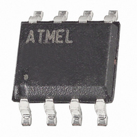
AT26DF321-SU Atmel, AT26DF321-SU Datasheet - Page 9

AT26DF321-SU
Manufacturer Part Number
AT26DF321-SU
Description
IC FLASH 32MBIT 66MHZ 8SOIC
Manufacturer
Atmel
Datasheet
1.AT26DF321-SU.pdf
(34 pages)
Specifications of AT26DF321-SU
Format - Memory
FLASH
Memory Type
DataFLASH
Memory Size
32M (16384 pages x 256 Bytes)
Speed
66MHz
Interface
SPI, 3-Wire Serial
Voltage - Supply
2.7 V ~ 3.6 V
Operating Temperature
-40°C ~ 85°C
Package / Case
8-SOIC (5.3mm Width), 8-SOP, 8-SOEIAJ
Lead Free Status / RoHS Status
Lead free / RoHS Compliant
Available stocks
Company
Part Number
Manufacturer
Quantity
Price
Part Number:
AT26DF321-SU
Manufacturer:
ATMEL/爱特梅尔
Quantity:
20 000
Figure 8-1.
Figure 8-2.
8.2
3633F–DFLASH–5/7/08
SCK
SO
CS
Block Erase
SI
Byte Program
Page Program
SCK
SO
CS
SI
MSB
HIGH-IMPEDANCE
0
0
0
1
A block of 4K-, 32K-, or 64K-bytes can be erased (all bits set to the logical “1” state) in a single
operation by using one of three different opcodes for the Block Erase command. An opcode of
20h is used for a 4K-byte erase, an opcode of 52h is used for a 32K-byte erase, and an opcode
of D8h is used for a 64K-byte erase. Before a Block Erase command can be started, the Write
Enable command must have been previously issued to the device to set the WEL bit of the Sta-
tus Register to a logical “1” state.
To perform a Block Erase, the CS pin must first be asserted and the appropriate opcode (20h,
52h, or D8h) must be clocked into the device. After the opcode has been clocked in, the three
address bytes specifying an address within the 4K-, 32K-, or 64K-byte block to be erased must
be clocked in. Any additional data clocked into the device will be ignored. When the CS pin is
deasserted, the device will erase the appropriate block. The erasing of the block is internally
self-timed and should take place in a time of t
Since the Block Erase command erases a region of bytes, the lower order address bits do not
need to be decoded by the device. Therefore, for a 4K-byte erase, address bits A11-A0 will be
ignored by the device and their values can be either a logical “1” or “0”. For a 32K-byte erase,
address bits A14-A0 will be ignored, and for a 64K-byte erase, address bits A15-A0 will be
ignored by the device. Despite the lower order address bits not being decoded by the device, the
complete three address bytes must still be clocked into the device before the CS pin is deas-
serted; otherwise, the device will abort the operation and no erase operation will be performed.
0
2
OPCODE
0
HIGH-IMPEDANCE
MSB
3
0
0
0
4
0
1
0
5
0
2
OPCODE
1
6
0
3
0
7
0
MSB
4
A
ADDRESS BITS A23-A0
8
0
5
A
9
1
6
A
0
7
MSB
A
8
A
A
29 30
9
ADDRESS BITS A23-A0
A
A
10 11
A
A
31 32
MSB
A
D
12
A
D
33
DATA IN BYTE 1
D
34
D
35
A
29 30
D
BLKE
36
A
D
37 38
A
.
31 32
D
MSB
D
D
39
D
33
D
34
DATA IN
D
35
MSB
D
D
36
D
DATA IN BYTE n
D
37 38
D
D
D
D
39
D
D
AT26DF321
D
D
9


