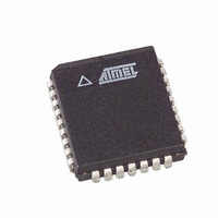
AT28C010-15JU Atmel, AT28C010-15JU Datasheet

AT28C010-15JU
Specifications of AT28C010-15JU
Available stocks
Related parts for AT28C010-15JU
AT28C010-15JU Summary of contents
Page 1
... When the device is deselected, the CMOS standby current is less than 200 µA. The AT28C010 is accessed like a Static RAM for the read or write cycle without the need for external components. The device contains a 128-byte page register to allow writing 128 bytes simultaneously ...
Page 2
... PDIP Top View 2.3 32-lead PLCC Top View 32 OE A10 I/ I/ I/ GND I/O0 I/ Note: PLCC package pin 1 is Don’t Connect. AT28C010 VCC A16 A15 A12 4 29 A14 A13 A11 A10 I/O7 ...
Page 3
... Read The AT28C010 is accessed like a Static RAM. When CE and OE are low and WE is high, the data stored at the memory location determined by the address pins is asserted on the outputs. The outputs are put in the high impedance state when either high. This dual-line control gives designers flexibility in preventing bus contention in their system ...
Page 4
... After writing the 3-byte command sequence and after t protected against inadvertent write operations. It should be noted, that once protected the host may still perform a byte or page write to the AT28C010. This is done by preceding the data to be written by the same 3-byte command sequence used to enable SDP. ...
Page 5
... MHz OUT -400 µ -100 µ 4. AT28C010 AT28C010-15 -40°C - 85°C 5V ± 10 High High Z Stresses beyond those listed under “Absolute Maximum Ratings” may cause permanent dam- age to the device. This is a stress rating only and functional operation of the device at these or any ...
Page 6
... whichever occurs first ( This parameter is characterized and is not 100% tested. AT28C010 6 AT28C010-12 Min (1)(2)(3)( after the address transition without impact on t ACC after the falling edge of CE without impact pF). L AT28C010-15 Max Min Max 120 150 120 150 ACC after an address change CE ...
Page 7
... Input Test Waveforms and Measurement Level 12. Output Test Load 13. Pin Capacitance ( MHz 25°C Symbol Typ OUT Note: 1. This parameter is characterized and is not 100% tested. 0353G–PEEPR–10/ < Max 10 12 AT28C010 Units Conditions OUT 7 ...
Page 8
... OES t Address Hold Time AH t Chip Select Set-up Time CS t Chip Select Hold Time CH t Write Pulse Width ( Data Set-up Time Data, OE Hold Time DH OEH 15. AC Write Waveforms 15.1 WE Controlled 15.2 CE Controlled AT28C010 8 Min Max Units 100 0353G–PEEPR–10/06 ...
Page 9
... A7 through A16 must specify the same page address during each high to low transition of WE (or CE must be high only when WE and CE are both low. 18. Chip Erase Waveforms = 5 µsec (min msec (min 12.0V ± 0. 0353G–PEEPR–10/06 Min 100 50 (1)(2) AT28C010 Max Units 150 µ ...
Page 10
... After the command sequence has been issued and a page write operation follows, the page address inputs (A7 - A16) must be the same for each high to low transition of WE (or CE must be high only when WE and CE are both low. AT28C010 10 20. Software Data Protection Disable Algorithm ...
Page 11
... Toggle Bit Waveforms Notes: 1. Toggling either both OE and CE will operate toggle bit. 2. Beginning and ending state of I/O6 will vary. 3. Any address location may be used but the address should not vary. 0353G–PEEPR–10/06 (1) Min (1) Min 150 AT28C010 Typ Max Typ Max ...
Page 12
... AT28C010(E)-12JI AT28C010(E)-12PI AT28C010(E)-12TI AT28C010(E)-15JI AT28C010(E)-15PI AT28C010(E)-15TI 13. Ordering Code AT28C010-12JU AT28C010-12TU AT28C010(E)-12JU AT28C010(E)-12PU AT28C010(E)-12TU AT28C010-15JU AT28C010-15TU AT28C010(E)-15JU AT28C010(E)-15PU AT28C010(E)-15TU Package Type Options Package Operation Range 32J 32P6 32T Industrial (-40° to 85° C) ...
Page 13
... The following table lists standard Atmel products that can be ordered. Device Numbers Speed AT28C010 12 AT28C010E 12 AT28C010 15 AT28C010E 15 28. Die Products Reference Section: Parallel EEPROM Die Products 0353G–PEEPR–10/06 Package and Temperature Combinations JI, JU, PI, TI, TU, PU JI, PI, TI, JU, PU, TU JI, JU, PI, TI, TU, PU JI, PI, TI, JU, PU, TU AT28C010 13 ...
Page 14
... Allowable protrusion is .010"(0.254 mm) per side. Dimension D1 and E1 include mold mismatch and are measured at the extreme material condition at the upper or lower parting line. 3. Lead coplanarity is 0.004" (0.102 mm) maximum. 2325 Orchard Parkway San Jose, CA 95131 R AT28C010 14 1.14(0.045) X 45˚ PIN NO. 1 IDENTIFIER E1 E ...
Page 15
... A1 0.381 – D 41.783 – E 15.240 – E1 13.462 – B 0.356 – B1 1.041 – L 3.048 – C 0.203 – eB 15.494 – e 2.540 TYP DRAWING NO. AT28C010 MAX NOTE 4.826 – 42.291 Note 1 15.875 13.970 Note 1 0.559 1.651 3.556 0.381 17.526 09/28/01 REV. 32P6 B 15 ...
Page 16
... E Notes: 1. This package conforms to JEDEC reference MO-142, Variation BD. 2. Dimensions D1 and E do not include mold protrusion. Allowable protrusion 0.15 mm per side and 0.25 mm per side. 3. Lead coplanarity is 0.10 mm maximum. 2325 Orchard Parkway San Jose, CA 95131 R AT28C010 16 PIN SEATING PLANE A1 TITLE ...
Page 17
... Disclaimer: The information in this document is provided in connection with Atmel products. No license, express or implied, by estoppel or otherwise, to any intellectual property right is granted by this document or in connection with the sale of Atmel products. EXCEPT AS SET FORTH IN ATMEL’S TERMS AND CONDI- TIONS OF SALE LOCATED ON ATMEL’S WEB SITE, ATMEL ASSUMES NO LIABILITY WHATSOEVER AND DISCLAIMS ANY EXPRESS, IMPLIED OR STATUTORY WARRANTY RELATING TO ITS PRODUCTS INCLUDING, BUT NOT LIMITED TO, THE IMPLIED WARRANTY OF MERCHANTABILITY, FITNESS FOR A PARTICULAR PURPOSE, OR NON-INFRINGEMENT ...


