AT28C010-20UM/883 Atmel, AT28C010-20UM/883 Datasheet
AT28C010-20UM/883
Specifications of AT28C010-20UM/883
Available stocks


Related parts for AT28C010-20UM/883

AT28C010-20UM/883 Summary of contents
Page 1
... A10 I/O5 I/ I/O4 GND 16 17 I/O3 32 LCC Top View I/ LCC Top View Top View 39 A13 A11 A10 29 CE AT28C010 Mil 1-Megabit (128K x 8) Paged Parallel EEPROMs AT28C010 Military (continued) 29 A14 28 A13 A11 A10 I/O7 PGA 0010F–PEEPR–02/10 ...
Page 2
... When the device is deselected, the CMOS standby current is less than 300 μA. The AT28C010 is accessed like a Static RAM for the read or write cycle without the need for external components. The device contains a 128-byte page register to allow writing 128- bytes simultaneously ...
Page 3
... After writing the 3-byte command sequence and after t protected against inadvertent write operations. It should be noted, that once protected the host may still perform a byte or page write to the AT28C010. This is done by preceding the data to be written by the same 3-byte command sequence used to enable SDP. ...
Page 4
... Once set, SDP will remain active unless the disable command sequence is issued. Power transi- tions do not disable SDP and SDP will protect the AT28C010 during power-up and power-down conditions. All command sequences must conform to the page write timing specifications. The data in the enable and disable command sequences is not written to the device and the memory addresses used in the sequence may be written with data in either a byte or page write opera- tion ...
Page 5
... specified from wichever occurs first ( pF This parameter is characterized and is not 100% tested de-asserted, it must remain de-asserted for at least 50ns during read operations other- wise incorrect data may be read. AT28C010 Military Min Max 2.0 0.45 2.4 4,2 AT28C010-20 ...
Page 6
... Address Hold Time AH t Data Set-up Time DS t Data Hold Time DH t Write Pulse Width WP t Byte Load Cycle Time BLC t Write Pulse Width High WPH AT28C010 Military 6 Max This parameter is 100% characterized and is not 100% tested. Units Conditions OUT Min ...
Page 7
... Page Mode Characteristics Symbol Parameter Address, OE Set-up Time AS OES t Address Hold Time AH t Chip Select Set-up Time CS t Chip Select Hold Time CH t Write Pulse Width ( Data Set-up Time Data, OE Hold Time DH OEH 0010F–PEEPR–02/10 AT28C010 Military Min Max Units 100 ...
Page 8
... Page Mode Write Waveforms Notes: AT28C010 Military through A16 must specify the page address during each high to low transition of WE (or CE must be high only when WE and CE are both low. (1)(2) 0010F–PEEPR–02/10 ...
Page 9
... Data Format: I/O7 - I/O0 (Hex); Address Format: A14 - A0 (Hex). 2. Write Protect state will be activated at end of write even if no other data is loaded. 3. Write Protect state will be deactivated at end of write period even if no other data if loaded 128 bytes of data are loaded. AT28C010 Military (1) (2) WRITES ENABLED (4) ...
Page 10
... Software Data Protection Disable Algorithm Software Protected Program Cycle Waveform Notes: AT28C010 Military 10 LOAD DATA AA TO ADDRESS 5555 LOAD DATA 55 TO ADDRESS 2AAA LOAD DATA 80 TO ADDRESS 5555 LOAD DATA AA TO ADDRESS 5555 LOAD DATA 55 TO ADDRESS 2AAA LOAD DATA 20 TO ...
Page 11
... These parameters are characterized and not 100% tested. 2. See AC Read Characteristics. (1)(2)(3) 1. Toggling either both OE and CE will operate toggle bit. 2. Beginning and ending state of I/O6 will vary. 3. Any addres location may be used but the address should not vary. AT28C010 Military Min Typ Max 10 10 ...
Page 12
... AT28C010(E)-12EM/883 AT28C010-12FM/883 AT28C010(E)-12LM/883 AT28C010(E)-12UM/883 AT28C010(E)-15DM/883 AT28C010(E)-15EM/883 AT28C010-15FM/883 AT28C010(E)-15LM/883 AT28C010(E)-15UM/883 AT28C010-20DM/883 AT28C010-20EM/883 AT28C010-20FM/883 AT28C010-20LM/883 AT28C010-20UM/883 AT28C010-25DM/883 AT28C010-25EM/883 AT28C010-25FM/883 AT28C010-25LM/883 AT28C010-25UM/883 1. See Valid Part Number table below. Package Type Options Package Operation Range 32D6 Military/883C 32L ...
Page 13
... MZX 5962-38267 03 MYX 5962-38267 03 MTX 5962-38267 01 MXX 5962-38267 01 MUX 5962-38267 01 MZX 5962-38267 01 MYX 5962-38267 01 MTX 1. See Valid Part Number table below. Package Type AT28C010 Military Package Operation Range 32D6 Military/883C 32F Class B, Fully Compliant 44L (-55°C to 125°C) 30U 32D6 ...
Page 14
... AT28C010 20 AT28C010 25 AT28C010 – Die Products Reference Section: Parallel EEPROM Die Products AT28C010 Military 14 Options Package and Temperature Combinations DM/883, EM/883, FM/883, LM/883, UM/883 DM/883, EM/883, LM/883, UM/883 DM/883, EM/883, FM/883, LM/883, UM/883 DM/883, EM/883, LM/883, UM/883 DM/883, EM/883, FM/883, LM/883, UM/883 ...
Page 15
Packaging Information 32D6, 32-Lead, 0.600" Wide, Non-Windowed, Ceramic Dual inline Package (Cerdip) Dimensions in Inches and (Millimeters) MIL-STD-1835 D-16 CONFIG A 42.70(1.68) 41.70(1.64) 38.10(1.500) REF 5.72(0.225) MAX SEATING PLANE 5.08(0.200) 3.18(0.125) 1.65(0.065) 1.14(0.045) 2.54(0.100)BSC 15.70(0.620) 15.00(0.590) 0º~ 15º REF 0.381(0.015) ...
Page 16
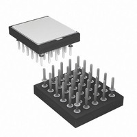
Packaging Information 30U, 30-Pin, Ceramic Pin Grid Array (PGA) Dimensions in Inches and (Millimeters) 13.74(0.541) 2.57(0.101) 13.36(0.526) 2.06(0.081) 16.18(0.637) 15.82(0.623) 14.17(0.558) 13.77(0.542) 2.54(0.100) TYP 16.71(0.658) 12.70(0.500) TYP 16.31(0.642) 2.54(0.100) TYP 10.41(0.410) 9.91(0.390) 0010F–PEEPR–02/10 7.26(0.286) 6.50(0.256) 1.40(0.055) 1.14(0.045) 0.58(0.023) 0.43(0.017) 3.12(0.123) ...
Page 17
... Disclaimer: The information in this document is provided in connection with Atmel products. No license, express or implied, by estoppel or otherwise, to any intellectual property right is granted by this document or in connection with the sale of Atmel products. EXCEPT AS SET FORTH IN ATMEL’S TERMS AND CONDI- TIONS OF SALE LOCATED ON ATMEL’S WEB SITE, ATMEL ASSUMES NO LIABILITY WHATSOEVER AND DISCLAIMS ANY EXPRESS, IMPLIED OR STATUTORY WARRANTY RELATING TO ITS PRODUCTS INCLUDING, BUT NOT LIMITED TO, THE IMPLIED WARRANTY OF MERCHANTABILITY, FITNESS FOR A PARTICULAR PURPOSE, OR NON-INFRINGEMENT ...