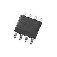
M25P05-AVMP6G NUMONYX, M25P05-AVMP6G Datasheet - Page 33

M25P05-AVMP6G
Manufacturer Part Number
M25P05-AVMP6G
Description
IC FLASH 512KBIT 50MHZ 8VFQFPN
Manufacturer
NUMONYX
Series
Forté™r
Datasheet
1.M25P05-AVMN6P.pdf
(52 pages)
Specifications of M25P05-AVMP6G
Format - Memory
FLASH
Memory Type
FLASH
Memory Size
512K (64K x 8)
Speed
50MHz
Interface
SPI, 3-Wire Serial
Voltage - Supply
2.7 V ~ 3.6 V
Operating Temperature
-40°C ~ 85°C
Package / Case
8-VFQFN, 8-VFQFPN
Memory Configuration
64K X 8
Ic Interface Type
Serial, SPI
Clock Frequency
50MHz
Supply Voltage Range
2.7V To 3.6V
Memory Case Style
VDFPN
No. Of Pins
8
Lead Free Status / RoHS Status
Lead free / RoHS Compliant
Available stocks
Company
Part Number
Manufacturer
Quantity
Price
Company:
Part Number:
M25P05-AVMP6G
Manufacturer:
Micron Technology Inc
Quantity:
10 000
Part Number:
M25P05-AVMP6G
Manufacturer:
MICRON
Quantity:
20 000
M25P05-A
6.12
Release from deep power-down and read electronic
signature (RES)
To take the device out of deep power-down mode, the release from deep power-down and
read electronic signature (RES) instruction must be issued. No other instruction must be
issued while the device is in deep power-down mode.
The instruction can also be used to read, on Serial Data output (Q), the 8-bit electronic
signature, whose value for the M25P05-A is 05h.
Except while an erase, program or write status register cycle is in progress, the release from
deep power-down and read electronic signature (RES) instruction always provides access
to the 8-bit electronic signature of the device, and can be applied even if the deep power-
down mode has not been entered.
Any release from deep power-down and read electronic signature (RES) instruction while an
erase, program or write status register cycle is in progress, is not decoded, and has no
effect on the cycle that is in progress.
The device is first selected by driving Chip Select (S) Low. The instruction code is followed
by 3 dummy bytes, each bit being latched-in on Serial Data input (D) during the rising edge
of Serial Clock (C). Then, the 8-bit electronic signature, stored in the memory, is shifted out
on Serial Data output (Q), each bit being shifted out during the falling edge of Serial Clock
(C).
The instruction sequence is shown in
The release from deep power-down and read electronic signature (RES) instruction is
terminated by driving Chip Select (S) High after the electronic signature has been read at
least once. Sending additional clock cycles on Serial Clock (C), while Chip Select (S) is
driven Low, cause the electronic signature to be output repeatedly.
When Chip Select (S) is driven High, the device is put in the standby power mode. If the
device was not previously in the deep power-down mode, the transition to the standby power
mode is immediate. If the device was previously in the deep power-down mode, though, the
transition to the standby power mode is delayed by t
High for at least t
device waits to be selected, so that it can receive, decode and execute instructions.
Driving Chip Select (S) High after the 8-bit instruction byte has been received by the device,
but before the whole of the 8-bit electronic signature has been transmitted for the first time
(as shown in
device was not previously in the deep power-down mode, the transition to the standby power
mode is immediate. If the device was previously in the deep power-down mode, though, the
transition to the standby power mode is delayed by t
High for at least t
device waits to be selected, so that it can receive, decode and execute instructions.
Figure
RES2
RES1
19), still ensures that the device is put into standby power mode. If the
(max), as specified in
(max), as specified in
Figure 18.
Table 15.
Table 15.
RES2
RES1
Once in the standby power mode, the
Once in the standby power mode, the
, and Chip Select (S) must remain
, and Chip Select (S) must remain
Instructions
33/52


