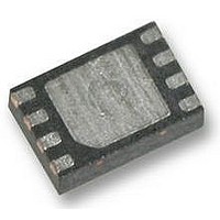
M25P20-VMP6G NUMONYX, M25P20-VMP6G Datasheet - Page 16

M25P20-VMP6G
Manufacturer Part Number
M25P20-VMP6G
Description
IC FLASH 2MBIT 50MHZ 8VFQFPN
Manufacturer
NUMONYX
Series
Forté™r
Specifications of M25P20-VMP6G
Format - Memory
FLASH
Memory Type
FLASH
Memory Size
2M (256K x 8)
Speed
50MHz
Interface
SPI, 3-Wire Serial
Voltage - Supply
2.7 V ~ 3.6 V
Operating Temperature
-40°C ~ 85°C
Package / Case
8-VFQFN, 8-VFQFPN
Clock Frequency
50MHz
Supply Voltage Range
2.7V To 3.6V
Memory Case Style
VDFPN
No. Of Pins
8
Base Number
25
Frequency
50MHz
Ic Generic Number
25P20
Memory Configuration
256K X 8
Interface Type
Serial, SPI
Rohs Compliant
Yes
Lead Free Status / RoHS Status
Lead free / RoHS Compliant
Available stocks
Company
Part Number
Manufacturer
Quantity
Price
Company:
Part Number:
M25P20-VMP6G
Manufacturer:
Micron Technology Inc
Quantity:
10 000
Part Number:
M25P20-VMP6G
Manufacturer:
ST
Quantity:
20 000
Company:
Part Number:
M25P20-VMP6GB
Manufacturer:
MICRON
Quantity:
5 600
Instructions
6
16/50
Instructions
All instructions, addresses and data are shifted in and out of the device, most significant bit
first.
Serial Data Input (D) is sampled on the first rising edge of Serial Clock (C) after Chip Select
(S) is driven Low. Then, the one-byte instruction code must be shifted in to the device, most
significant bit first, on Serial Data Input (D), each bit being latched on the rising edges of
Serial Clock (C).
The instruction set is listed in
Every instruction sequence starts with a one-byte instruction code. Depending on the
instruction, this might be followed by address bytes, or by data bytes, or by both or none.
Chip Select (S) must be driven High after the last bit of the instruction sequence has been
shifted in.
In the case of a Read Data Bytes (READ), Read Data Bytes at Higher Speed (Fast_Read),
Read Identification (RDID), Read Status Register (RDSR) or Release from Deep Power-
down, and Read Electronic Signature (RES) instruction, the shifted-in instruction sequence
is followed by a data-out sequence. Chip Select (S) can be driven High after any bit of the
data-out sequence is being shifted out.
In the case of a Page Program (PP), Sector Erase (SE), Bulk Erase (BE), Write Status
Register (WRSR), Write Enable (WREN), Write Disable (WRDI) or Deep Power-down (DP)
instruction, Chip Select (S) must be driven High exactly at a byte boundary, otherwise the
instruction is rejected, and is not executed. That is, Chip Select (S) must driven High when
the number of clock pulses after Chip Select (S) being driven Low is an exact multiple of
eight.
All attempts to access the memory array during a Write Status Register cycle, Program
cycle or Erase cycle are ignored, and the internal Write Status Register cycle, Program
cycle or Erase cycle continues unaffected.
Table
4.
M25P20


