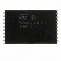
M28W320FCT70N6E NUMONYX, M28W320FCT70N6E Datasheet - Page 13

M28W320FCT70N6E
Manufacturer Part Number
M28W320FCT70N6E
Description
IC FLASH 32MBIT 70NS 48TSOP
Manufacturer
NUMONYX
Datasheet
1.M28W320FCB70ZB6F.pdf
(69 pages)
Specifications of M28W320FCT70N6E
Format - Memory
FLASH
Memory Type
FLASH - Nor
Memory Size
32M (2M x 16)
Speed
70ns
Interface
Parallel
Voltage - Supply
2.7 V ~ 3.6 V
Operating Temperature
-40°C ~ 85°C
Package / Case
48-TSOP
Memory Configuration
2M X 16
Ic Interface Type
Parallel
Access Time
70ns
Supply Voltage Range
2.7V To 3.6V
Memory Case Style
TSOP
No. Of Pins
48
Lead Free Status / RoHS Status
Lead free / RoHS Compliant
Available stocks
Company
Part Number
Manufacturer
Quantity
Price
Company:
Part Number:
M28W320FCT70N6E
Manufacturer:
MICRON
Quantity:
3 000
Company:
Part Number:
M28W320FCT70N6E
Manufacturer:
Numonyx
Quantity:
9 792
Part Number:
M28W320FCT70N6E
Manufacturer:
ST
Quantity:
20 000
2.7
2.8
2.9
2.10
2.11
Reset (RP)
The Reset input provides a hardware reset of the memory. When Reset is at V
memory is in reset mode: the outputs are high impedance and the current consumption is
minimized. After Reset all blocks are in the Locked state. When Reset is at V
in normal operation. Exiting reset mode the device enters read array mode, but a negative
transition of Chip Enable or a change of the address is required to ensure valid data outputs.
V
V
power supply for all operations (Read, Program and Erase).
V
V
independently from V
V
V
voltage range applied to the pin. The Supply Voltage V
V
If V
a voltage lower than V
V
sampled at the beginning of a Program or Erase; a change in its value after the operation
has started does not have any effect on Program or Erase, however for Double or
Quadruple Word Program the results are uncertain.
If V
be stable until the Program/Erase algorithm is completed (see
V
V
Note: Each device in a system should have V
capacitor close to the pin. See
widths should be sufficient to carry the required V
DD
DDQ
PP
PP
PP
SS
DD
DDQ
PP
SS
PP
PP
is both a control input and a power supply pin. The two functions are selected by the
can be applied in any order.
> V
is the reference for all voltage measurements.
provides the power supply to the internal core of the memory device. It is the main
provides the power supply to the I/O pins and enables all Outputs to be powered
Program supply voltage
is kept in a low voltage range (0V to 3.6V) V
is in the range 11.4V to 12.6V it acts as a power supply pin. In this condition V
ground
supply voltage
PP1
supply voltage
enables these functions (see
DD
PPLK
. V
DDQ
gives an absolute protection against program or erase, while
Figure 7: AC Measurement Load
can be tied to V
Table 15: DC
DD
DD
, V
PP
PP
or can use a separate supply.
DDQ
program and erase currents.
is seen as a control input. In this case
DD
Characteristics). V
and V
and the Program Supply Voltage
PP
Table 17
decoupled with a 0.1μF
Circuit. The PCB trace
and
PP
IH
Table
is only
, the device is
IL
, the
18).
PP
must
13/69


