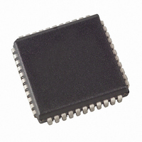
AT29C1024-70JI Atmel, AT29C1024-70JI Datasheet - Page 3

AT29C1024-70JI
Manufacturer Part Number
AT29C1024-70JI
Description
IC FLASH 1MBIT 70NS 44PLCC
Manufacturer
Atmel
Datasheet
1.AT29C1024-70JC.pdf
(16 pages)
Specifications of AT29C1024-70JI
Format - Memory
FLASH
Memory Type
FLASH
Memory Size
1M (64K x 16)
Speed
70ns
Interface
Parallel
Voltage - Supply
4.5 V ~ 5.5 V
Operating Temperature
-40°C ~ 85°C
Package / Case
44-PLCC
Lead Free Status / RoHS Status
Contains lead / RoHS non-compliant
Available stocks
Company
Part Number
Manufacturer
Quantity
Price
Company:
Part Number:
AT29C1024-70JI
Manufacturer:
ATM
Quantity:
2 200
Company:
Part Number:
AT29C1024-70JI
Manufacturer:
ATM
Quantity:
3 500
Company:
Part Number:
AT29C1024-70JI
Manufacturer:
AD
Quantity:
476
Company:
Part Number:
AT29C1024-70JI
Manufacturer:
FSC
Quantity:
35
Part Number:
AT29C1024-70JI
Manufacturer:
ATMEL/爱特梅尔
Quantity:
20 000
After setting SDP, any attempt to write to the device without
the 3-word command sequence will start the internal write
timers. No data will be written to the device; however, for
the duration of t
polling operation.
After the software data protection’s 3-word command code
is given, a sector of data is loaded into the device using the
sector programming timing specifications.
HARDWARE DATA PROTECTION: Hardware features
protect against inadvertent programs to the AT29C1024 in
the following ways: (a) V
(typical), the program function is inhibited; (b) V
delay—once V
device will automatically time out 5 ms (typical) before pro-
gramming; (c) Program inhibit—holding any one of OE low,
CE high or WE high inhibits program cycles; and (d) Noise
filter—pulses of less than 15 ns (typical) on the WE or CE
inputs will not initiate a program cycle.
PRODUCT IDENTIFICATION: The product identification
mode identifies the device and manufacturer as Atmel. It
may be accessed by hardware or software operation. The
hardware operation mode can be used by an external pro-
grammer to identify the correct programming algorithm for
the Atmel product. In addition, users may wish to use the
software product identification mode to identify the part (i.e.
using the device code), and have the system software use
the appropriate sector size for program operations. In this
Absolute Maximum Ratings*
Temperature Under Bias ................................ -55 C to +125 C
Storage Temperature ..................................... -65 C to +150 C
All Input Voltages (including NC Pins)
with Respect to Ground ...................................-0.6V to +6.25V
All Output Voltages
with Respect to Ground .............................-0.6V to V
Voltage on OE
with Respect to Ground ...................................-0.6V to +13.5V
CC
WC
has reached the V
, a read operation will effectively be a
CC
sense—if V
CC
CC
sense level, the
is below 3.8V
CC
CC
power on
+ 0.6V
manner, the user can have a common board design for var-
ious Flash densities and, with each density’s sector size in
a memory map, have the system software apply the appro-
priate sector size.
For details, see Operating Modes (for hardware operation)
or Software Product Identification. The manufacturer and
device code is the same for both modes.
DATA POLLING: The AT29C1024 features DATA polling
to indicate the end of a program cycle. During a program
cycle an attempted read of the last word loaded will result
in the complement of the loaded data on I/O7 and I/O15.
Once the program cycle has been completed, true data is
valid on all outputs and the next cycle may begin. DATA
polling may begin at any time during the program cycle.
T O G G L E B I T :
AT29C1024 provides another method for determining the
end of a program or erase cycle. During a program or erase
operation, successive attempts to read data from the
device will result in I/O6 and I/O14 toggling between one
and zero. Once the program cycle has completed, I/O6 and
I/O14 will stop toggling and valid data will be read. Examin-
ing the toggle bit may begin at any time during a program
cycle.
OPTIONAL CHIP ERASE MODE: The entire device can
be erased by using a 6-byte software code. Please see
Software Chip Erase application note for details.
*NOTICE:
Stresses beyond those listed under “Absolute
Maximum Ratings” may cause permanent dam-
age to the device. This is a stress rating only and
functional operation of the device at these or any
other conditions beyond those indicated in the
operational sections of this specification is not
implied. Exposure to absolute maximum rating
conditions for extended periods may affect
device reliability.
I n a d d i t i o n t o D A T A p o l l i n g t h e
3


