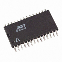
AT45DB021B-RC Atmel, AT45DB021B-RC Datasheet - Page 7

AT45DB021B-RC
Manufacturer Part Number
AT45DB021B-RC
Description
IC FLASH 2MBIT 20MHZ 28SOIC
Manufacturer
Atmel
Datasheet
1.AT45DB021B-RC.pdf
(32 pages)
Specifications of AT45DB021B-RC
Format - Memory
FLASH
Memory Type
DataFLASH
Memory Size
2M (1024 pages x 264 bytes)
Speed
20MHz
Interface
SPI, 3-Wire Serial
Voltage - Supply
2.7 V ~ 3.6 V
Operating Temperature
0°C ~ 70°C
Package / Case
28-SOIC (7.5mm Width)
Lead Free Status / RoHS Status
Contains lead / RoHS non-compliant
5.2.4
5.2.5
5.2.6
1937J–DFLSH–9/05
Page Erase
Block Erase
Main Memory Page Program through Buffer
The optional Page Erase command can be used to individually erase any page in the main
memory array allowing the Buffer to Main Memory Page Program without Built-in Erase com-
mand to be utilized at a later time. To perform a Page Erase, an opcode of 81H must be loaded
into the device, followed by five reserved bits, ten address bits (PA9-PA0), and nine don’t care
bits. The ten address bits are used to specify which page of the memory array is to be erased.
When a low-to-high transition occurs on the CS pin, the part will erase the selected page to 1s.
The erase operation is internally self-timed and should take place in a maximum time of t
ing this time, the status register will indicate that the part is busy.
A block of eight pages can be erased at one time allowing the Buffer to Main Memory Page Pro-
gram without Built-in Erase command to be utilized to reduce programming times when writing
large amounts of data to the device. To perform a Block Erase, an opcode of 50H must be
loaded into the device, followed by five reserved bits, seven address bits (PA9 -PA3), and 12
don’t care bits. The seven address bits are used to specify which block of eight pages is to be
erased. When a low-to-high transition occurs on the CS pin, the part will erase the selected
block of eight pages to 1s. The erase operation is internally self-timed and should take place in a
maximum time of t
Table 5-2.
This operation is a combination of the Buffer Write and Buffer to Main Memory Page Program
with Built-in Erase operations. Data is first shifted into buffer 1 or buffer 2 from the SI pin and
then programmed into a specified page in the main memory. To initiate the operation, an 8-bit
opcode (82H for buffer 1 or 85H for buffer 2) must be followed by the five reserved bits and 20
address bits. The 10 most-significant address bits (PA9-PA0) select the page in the main mem-
ory where data is to be written, and the next nine address bits (BFA8-BFA0) select the first byte
in the buffer to be written. After all address bits are shifted in, the part will take data from the SI
pin and store it in one of the data buffers. If the end of the buffer is reached, the device will wrap
around back to the beginning of the buffer. When there is a low-to-high transition on the CS pin,
the part will first erase the selected page in main memory to all 1s and then program the data
stored in the buffer into the specified page in the main memory. Both the erase and the program-
ming of the page are internally self-timed and should take place in a maximum of time t
During this time, the status register will indicate that the part is busy.
PA9
0
0
0
0
1
1
1
1
•
•
•
PA8
0
0
0
0
1
1
1
1
•
•
•
Block Erase Addressing
BE
PA7
. During this time, the status register will indicate that the part is busy.
0
0
0
0
1
1
1
1
•
•
•
PA6
0
0
0
0
1
1
1
1
•
•
•
PA5
0
0
0
0
1
1
1
1
•
•
•
PA4
0
0
1
1
0
0
1
1
•
•
•
PA3
0
1
0
1
0
1
0
1
•
•
•
PA2
X
X
X
X
X
X
X
X
•
•
•
PA1
AT45DB021B
X
X
X
X
X
X
X
X
•
•
•
PA0
X
X
X
X
X
X
X
X
•
•
•
Block
PE
124
125
126
127
0
1
2
3
•
•
•
. Dur-
EP
7
.


