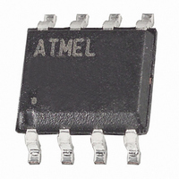
AT24C64N-10SC-1.8 Atmel, AT24C64N-10SC-1.8 Datasheet

AT24C64N-10SC-1.8
Specifications of AT24C64N-10SC-1.8
Available stocks
Related parts for AT24C64N-10SC-1.8
AT24C64N-10SC-1.8 Summary of contents
Page 1
... Description The AT24C32/64 provides 32,768/65,536 bits of serial electrically erasable and pro- grammable read only memory (EEPROM) organized as 4096/8192 words of 8 bits each. The device’s cascadable feature allows devices to share a common 2- wire bus. The device is optimized for use in many industrial and commercial applica- tions where low power and low voltage operation are essential ...
Page 2
Absolute Maximum Ratings* Operating Temperature.................................. - +125 C Storage Temperature ..................................... - +150 C Voltage on Any Pin with Respect to Ground .....................................-1.0V to +7.0V Maximum Operating Voltage .......................................... 6.25V DC Output Current........................................................ 5.0 mA Block ...
Page 3
... WRITE PROTECT (WP): The write protect input, when tied to GND, allows normal write operations. When WP is tied high to V (8/16K bits) of memory are inhibited. If left unconnected internally pulled down to GND. AT24C32/64, 32K/64K SERIAL EEPROM: The 32K/64K is internally organized as 256 pages of 32 bytes each. Random word addressing requires a 12/13 bit data word address ...
Page 4
Pin Capacitance Applicable over recommended operating range from T Symbol Test Condition C Input/Output Capacitance (SDA) I/O C Input Capacitance ( Note: 1. This parameter is characterized and is not 100% tested. DC Characteristics Applicable ...
Page 5
AC Characteristics Applicable over recommended operating range from T pF (unless otherwise noted). Symbol Parameter f Clock Frequency, SCL SCL t Clock Pulse Width Low LOW t Clock Pulse Width High HIGH t Noise Suppression Time I t Clock Low ...
Page 6
... STOP bit and the completion of any internal operations. MEMORY RESET: After an interruption in protocol, power loss or system reset, any 2- wire part can be reset by following these steps: (a) Clock cycles, (b) look for SDA high in each cycle while SCL is high and then (c) create a start condition as SDA is high ...
Page 7
Bus Timing SCL: Serial Clock, SDA: Serial Data I/O Write Cycle Timing SCL: Serial Clock, SDA: Serial Data I/O SCL SDA 8th BIT WORDn Note: 1. The write cycle time t is the time from a valid stop condition of ...
Page 8
Data Validity Start and Stop Definition Output Acknowledge AT24C32/64 8 0336K–SEEPR–7/03 ...
Page 9
... A low-V resets the device to prevent data corruption in a noisy environment. DATA SECURITY: The AT24C32/64 has a hardware data protection scheme that allows the user to write protect the upper quadrant (8/16K bits) of memory when the WP pin ...
Page 10
... The address “roll over” during read is from the last byte of the last memory page, to the first byte of the first page. The address “roll over” during write is from the last byte of the current page to the first byte of the same page ...
Page 11
Figure 1. Device Address Figure 2. Byte Write Figure 3. Page Write Note DON’T CARE bits 2. † = DON’T CARE bits for the 32K 0336K–SEEPR–7/03 AT24C32/64 11 ...
Page 12
Figure 4. Current Address Read Figure 5. Random Read Note DON’T CARE bits Figure 6. Sequential Read AT24C32/64 12 0336K–SEEPR–7/03 ...
Page 13
AT24C32 Ordering Information Ordering Code AT24C32-10PI-2.7 AT24C32N-10SI-2.7 AT24C32W-10SI-2.7 AT24C32-10PI-1.8 AT24C32N-10SI-1.8 AT24C32W-10SI-1.8 Note: For 2.7V devices used in the 4.5V to 5.5V range, please refer to performance values in the AC and DC characteristics tables. 8P3 8-lead, 0.300” Wide, Plastic Dual ...
Page 14
... AT24C64 Ordering Information Ordering Code AT24C64-10PI-2.7 AT24C64N-10SI-2.7 AT24C64W-10SI-2.7 AT24C64-10TI-2.7 AT24C64-10PI-1.8 AT24C64N-10SI-1.8 AT24C64W-10SI-1.8 AT24C64-10TI-1.8 Note: For 2.7V devices used in the 4.5V to 5.5V range, please refer to performance values in the AC and DC characteristics tables. 8P3 8-lead, 0.300” Wide, Plastic Dual Inline Package (PDIP) 8S1 8-lead, 0.150” ...
Page 15
Packaging Information 8P3 – PDIP Top View PLCS Side View Notes: 1. This drawing is for general information only; refer to JEDEC Drawing MS-001, Variation BA for additional information. 2. Dimensions A and L are measured ...
Page 16
JEDEC SOIC 3 2 Top View e D Side View End View Note: This drawing is for general information only. Refer to JEDEC Drawing MS-012 for proper dimensions, tolerances, datums, etc. 2325 Orchard Parkway San ...
Page 17
EIAJ SOIC 1 N Top View Side View End View Notes: 1. This drawing is for general information only; refer to EIAJ Drawing EDR-7320 for additional information. 2. Mismatch of the upper ...
Page 18
TSSOP Pin 1 indicator this corner N Top View Side View Notes: 1. This drawing is for general information only. Refer to JEDEC Drawing MO-153, Variation AA, for proper dimensions, tolerances, datums, ...
Page 19
... No licenses to patents or other intellectual property of Atmel are granted by the Company in connection with the sale of Atmel products, expressly or by implication. Atmel’s products are not authorized for use as critical components in life support devices or systems. ...


