AT27BV1024-90VI Atmel, AT27BV1024-90VI Datasheet - Page 9
AT27BV1024-90VI
Manufacturer Part Number
AT27BV1024-90VI
Description
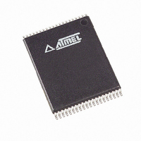
IC OTP 1MBIT 90NS 40VSOP
Manufacturer
Atmel
Datasheet
1.AT27BV1024-90JU.pdf
(14 pages)
Specifications of AT27BV1024-90VI
Format - Memory
EPROMs
Memory Type
OTP EPROM
Memory Size
1M (64K x 16)
Speed
90ns
Interface
Parallel
Voltage - Supply
2.7 V ~ 3.6 V, 4.5 V ~ 5.5 V
Operating Temperature
-40°C ~ 85°C
Package / Case
40-VSOP
Lead Free Status / RoHS Status
Contains lead / RoHS non-compliant
Other names
AT27BV102490VI
Available stocks
Company
Part Number
Manufacturer
Quantity
Price

Part Number:
AT27BV1024-90VI
Manufacturer:
ATMEL/爱特梅尔
Quantity:
20 000


15. DC Programming Characteristics
T
16. AC Programming Characteristics
T
Notes:
17. Atmel’s AT27BV1024 Integrated Product Identification Code
Note:
0631E–EPROM–12/07
A
A
Symbol
I
V
V
V
V
I
I
V
Symbol
t
t
t
t
t
t
t
t
t
t
t
t
Codes
Manufacturer
Device Type
LI
CC2
PP2
AS
CES
OES
DS
AH
DH
DFP
VPS
VCS
PW
OE
PRT
IL
IH
OL
OH
ID
= 25 ± 5° C, V
= 25 ± 5° C, V
1. V
2. This parameter is only sampled and is not 100% tested. Output Float is defined as the point where data is no longer driven –
3. Program Pulse width tolerance is 100 µsec ± 5%.
1. The AT27BV1024 has the same Product Identification Code as the AT27C1024. Both are programming compatible.
see timing diagram.
CC
Parameter
Input Load Current
Input Low Level
Input High Level
Output Low Voltage
Output High Voltage
V
V
A9 Product Identification Voltage
Parameter
Address Setup Time
CE Setup Time
OE Setup Time
Data Setup Time
Address Hold Time
Data Hold Time
OE High to Output Float Delay
V
V
PGM Program Pulse Width
Data Valid from OE
V
CC
PP
PP
CC
PP
must be applied simultaneously or before V
CC
CC
Pulse Rise Time During Programming
Supply Current
Setup Time
Supply Current (Program and Verify)
Setup Time
= 6.5 ± 0.25V, V
= 6.5 ± 0.25V, V
A0
0
1
O15-O8
PP
PP
= 13.0 ± 0.25V
= 13.0 ± 0.25V
(3)
0
0
(2)
O7
0
1
O6
Test Conditions
Input Rise and Fall Times:
Input Pulse Levels:
Input Timing Reference Level:
Output Timing Reference Level:
PP
0
1
and removed simultaneously or after V
I
Test Conditions
V
I
CE = PGM = V
OL
OH
IN
= 2.1 mA
= V
= -400 µA
O5
0
1
IL
(10% to 90%) 20 ns
Pins
, V
IH
(1)
0.45V to 2.4V
O4
1
1
0.8V to 2.0V
0.8V to 2.0V
IL
O3
1
0
11.5
Min
-0.6
2.0
2.4
O2
1
0
Min
95
50
2
2
2
2
0
2
0
2
2
PP
Limits
.
Limits
(1)
O1
1
0
V
AT27BV1024
CC
Max
12.5
±10
0.8
0.4
50
30
+ 0.1
Max
130
105
150
O0
0
1
Units
Units
001E
00F1
Data
mA
mA
Hex
µA
V
V
V
V
V
µs
µs
µs
µs
µs
µs
ns
µs
µs
µs
ns
ns
9
Related parts for AT27BV1024-90VI
Image
Part Number
Description
Manufacturer
Datasheet
Request
R

Part Number:
Description:
DEV KIT FOR AVR/AVR32
Manufacturer:
Atmel
Datasheet:

Part Number:
Description:
INTERVAL AND WIPE/WASH WIPER CONTROL IC WITH DELAY
Manufacturer:
ATMEL Corporation
Datasheet:
Part Number:
Description:
Low-Voltage Voice-Switched IC for Hands-Free Operation
Manufacturer:
ATMEL Corporation
Datasheet:
Part Number:
Description:
MONOLITHIC INTEGRATED FEATUREPHONE CIRCUIT
Manufacturer:
ATMEL Corporation
Datasheet:
Part Number:
Description:
AM-FM Receiver IC U4255BM-M
Manufacturer:
ATMEL Corporation
Datasheet:
Part Number:
Description:
Monolithic Integrated Feature Phone Circuit
Manufacturer:
ATMEL Corporation
Datasheet:
Part Number:
Description:
Multistandard Video-IF and Quasi Parallel Sound Processing
Manufacturer:
ATMEL Corporation
Datasheet:
Part Number:
Description:
High-performance EE PLD
Manufacturer:
ATMEL Corporation
Datasheet:
Part Number:
Description:
8-bit Flash Microcontroller
Manufacturer:
ATMEL Corporation
Datasheet:
Part Number:
Description:
2-Wire Serial EEPROM
Manufacturer:
ATMEL Corporation
Datasheet: