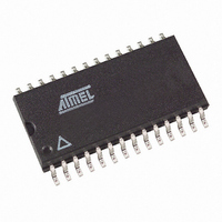
AT28LV64B-25SC Atmel, AT28LV64B-25SC Datasheet - Page 3

AT28LV64B-25SC
Manufacturer Part Number
AT28LV64B-25SC
Description
IC EEPROM 64KBIT 250NS 28SOIC
Manufacturer
Atmel
Datasheet
1.AT28LV64B-20JI.pdf
(12 pages)
Specifications of AT28LV64B-25SC
Format - Memory
EEPROMs - Parallel
Memory Type
EEPROM
Memory Size
64K (8K x 8)
Speed
250ns
Interface
Parallel
Voltage - Supply
3 V ~ 3.6 V
Operating Temperature
0°C ~ 70°C
Package / Case
28-SOIC (7.5mm Width)
Lead Free Status / RoHS Status
Contains lead / RoHS non-compliant
Other names
AT28LV64B25SC
Device Operation
READ: The AT28LV64B is accessed like a static RAM.
When CE and OE are low and WE is high, the data stored
at the memory location determined by the address pins is
asserted on the outputs. The outputs are put in the high
impedance state when either CE or OE is high. This dual-
line control gives designers flexibility in preventing bus con-
tention in their systems.
BYTE WRITE: A low pulse on the WE or CE input with CE
or WE low (respectively) and OE high initiates a write cycle.
The address is latched on the falling edge of CE or WE,
whichever occurs last. The data is latched by the first rising
edge of CE or WE. Once a byte write has been started, it
will automatically time itself to completion. Once a pro-
gramming operation has been initiated and for the duration
of t
tion.
PAGE WRITE: The page write operation of the AT28LV64B
allows 1 to 64 bytes of data to be written into the device
during a single internal programming period. A page write
operation is initiated in the same manner as a byte write;
the first byte written can then be followed by 1 to 63 addi-
tional bytes. Each successive byte must be written within
100 µs (t
exceeded, the AT28LV64B will cease accepting data and
commence the internal programming operation. All bytes
during a page write operation must reside on the same
page as defined by the state of the A6 to A12 inputs. For
each WE high to low transition during the page write opera-
tion, A6 to A12 must be the same.
The A0 to A5 inputs specify which bytes within the page are
to be written. The bytes may be loaded in any order and
may be altered within the same load period. Only bytes
which are specified for writing will be written; unnecessary
cycling of other bytes within the page does not occur.
DATA POLLING: The AT28LV64B features DATA Polling to
indicate the end of a write cycle. During a byte or page
write cycle an attempted read of the last byte written will
result in the complement of the written data to be presented
on I/O7. Once the write cycle has been completed, true
data is valid on all outputs, and the next write cycle may
begin. DATA Polling may begin at anytime during the write
cycle.
TOGGLE BIT: In addition to DATA Polling, the AT28LV64B
provides another method for determining the end of a write
cycle. During the write operation, successive attempts to
WC
, a read operation will effectively be a polling opera-
BLC
) of the previous byte. If the t
BLC
limit is
read data from the device will result in I/O6 toggling
between one and zero. Once the write has completed, I/O6
will stop toggling and valid data will be read. Reading the
toggle bit may begin at any time during the write cycle.
DATA PROTECTION: If precautions are not taken, inad-
vertent writes may occur during transitions of the host sys-
tem power supply. Atmel has incorporated both hardware
and software features that will protect the memory against
inadvertent writes.
HARDWARE PROTECTION: Hardware features protect
against inadvertent writes to the AT28LV64B in the follow-
ing ways: (a) V
1.8V (typical) the device will automatically time out 10 ms
(typical) before allowing a write; (b) write inhibit holding
any one of OE low, CE high or WE high inhibits write
cycles; and (c) noise filter pulses of less than 15 ns (typi-
cal) on the WE or CE inputs will not initiate a write cycle.
SOFTWARE DATA PROTECTION: A software-controlled
data protection feature has been implemented on the
AT28LV64B. Software data protection (SDP) helps prevent
inadvertent writes from corrupting the data in the device.
SDP can prevent inadvertent writes during power-up and
power-down as well as any other potential periods of sys-
tem instability.
The AT28LV64B can only be written using the software
data protection feature. A series of three write commands
to specific addresses with specific data must be presented
to the device before writing in the byte or page mode. The
same three write commands must begin each write opera-
tion. All software write commands must obey the page
mode write timing specifications. The data in the 3-byte
command sequence is not written to the device; the
addresses in the command sequence can be utilized just
like any other location in the device.
Any attempt to write to the device without the 3-byte
sequence will start the internal write timers. No data will be
written to the device; however, for the duration of t
operations will effectively be polling operations.
DEVICE IDENTIFICATION: An extra 64 bytes of EEPROM
memory are available to the user for device identification.
By raising A9 to 12V ± 0.5V and using address locations
7FC0H to 7FFFH, the additional bytes may be written to or
read from in the same manner as the regular memory
array.
CC
power-on delay—once V
CC
has reached
WC
, read
3


