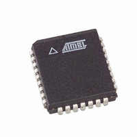
AT29C257-12JI Atmel, AT29C257-12JI Datasheet

AT29C257-12JI
Specifications of AT29C257-12JI
Available stocks
Related parts for AT29C257-12JI
AT29C257-12JI Summary of contents
Page 1
... Five-volt-only commands determine the operation of the device. Reading data out of the device is similar to reading from a static RAM. Reprogramming the AT29C257 is performed on a page basis; 64-bytes of data are loaded into the device and then simultaneously programmed. The contents of the entire device may be erased by using a 6-byte software code (although erasure before programming is not needed) ...
Page 2
... AT29C257 4-106 SOFTWARE DATA PROTECTION: led data protection feature is available on the AT29C257. Once the software protection is enabled a software algo- rithm must be issued to the device before a program may be performed. The software protection feature may be en- abled or disabled by the user; when shipped from Atmel, the software data protection feature is disabled ...
Page 3
... Device Operation (Continued) HARDWARE DATA PROTECTION: protect against inadvertent programs to the AT29C257 in the following ways: (a) V sense— (typical), the program function is inhibited. ( delay— once V has reached the V CC the device will automatically time out 5 ms (typical) before programming. (c) Program inhibit— holding any one of OE low, CE high or WE high inhibits program cycles. (d) Noise filter— ...
Page 4
... A14 = A14 = V 4. Manufacturer Code: 1F, Device Code See details under Software Product Identification Entry/Exit. Condition MHz OUT -400 -100 4. AT29C257-12 AT29C257 10% 5V 10 OUT High Z High Z X High Manufacturer Code ( Device Code Manufacturer Code IL ( Device Code IH Min Max Units ...
Page 5
... whichever occurs first pF). ACC after the falling 4. This parameter is characterized and is not 100% tested ACC OE . ACC (1) Typ Max AT29C257 AT29C257-12 AT29C257-15 Min Max Min Max 120 150 120 150 Output Test Load Units Conditions OUT Units ...
Page 6
... Address Hold Time AH t Chip Select Set-up Time CS t Chip Select Hold Time CH t Write Pulse Width ( Data Set-up Time Data, OE Hold Time DH OEH t Write Pulse Width High WPH AC Byte Load Waveforms WE Controlled CE Controlled AT29C257 4-110 Min Max 100 Units ...
Page 7
... Notes through A14 must specify the page address during each high to low transition of WE (or CE must be high when WE and CE are both low. Min 100 ( All bytes that are not loaded within the page being programmed will be indeterminate. AT29C257 Max Units 150 s ns ...
Page 8
... Software Protected Program Cycle Waveform Notes through A14 must specify the page address during each high to low transition of WE (or CE) after the software code has been entered must be high when WE and CE are both low. AT29C257 4-112 Software Data (1) Protection Disable Algorithm ...
Page 9
... Notes: 1. Toggling either both OE and CE will operate toggle bit. 2. Beginning and ending state of I/O6 will vary. (1) Min 0 10 (2) 0 (1) Min 0 10 (2) 150 0 3. Any address location may be used but the address should not vary. AT29C257 Typ Max Typ Max Units Units 4-113 ...
Page 10
... IL Manufacture Code is read for Device Code is read for The device does not remain in identification mode if powered down. 4. The device returns to standard operation mode. 5. Manufacturer Code: 1F Device Code: DC AT29C257 4-114 Software Product Identification Exit ENTER PRODUCT IDENTIFICATION ( MODE IL; (1) LOAD DATA AA ...
Page 11
... AT29C257 4-115 ...
Page 12
... Lead, Plastic J-Leaded Chip Carrier (PLCC) AT29C257 4-116 Ordering Code Package AT29C257-70JC 32J AT29C257-70JI 32J AT29C257-90JC 32J AT29C257-90JI 32J AT29C257-12JC 32J AT29C257-12JI 32J AT29C257-15JC 32J AT29C257-15JI 32J Package Type Operation Range Commercial ( Industrial (- Commercial ( Industrial (- Commercial ( Industrial (- Commercial ...


