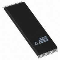
AT29LV512-25TI Atmel, AT29LV512-25TI Datasheet - Page 4

AT29LV512-25TI
Manufacturer Part Number
AT29LV512-25TI
Description
IC FLASH 512KBIT 250NS 32TSOP
Manufacturer
Atmel
Datasheet
1.AT29LV512-15JC.pdf
(15 pages)
Specifications of AT29LV512-25TI
Format - Memory
FLASH
Memory Type
FLASH
Memory Size
512K (64K x 8)
Speed
250ns
Interface
Parallel
Voltage - Supply
3 V ~ 3.6 V
Operating Temperature
-40°C ~ 85°C
Package / Case
32-TSOP
Lead Free Status / RoHS Status
Contains lead / RoHS non-compliant
Other names
AT29LV51225TI
Available stocks
Company
Part Number
Manufacturer
Quantity
Price
Company:
Part Number:
AT29LV512-25TI
Manufacturer:
ATMEL
Quantity:
657
4.3
4.4
4.5
4.6
4
Hardware Data Protection
Input Levels
Product Identification
DATA Polling
AT29LV512
The 128 bytes of data must be loaded into each sector. Any byte that is not loaded during the
programming of its sector will be erased to read FFh. Once the bytes of a sector are loaded into
the device, they are simultaneously programmed during the internal programming period. After
the first data byte has been loaded into the device, successive bytes are entered in the same
manner. Each new byte to be programmed must have its high-to-low transition on WE (or CE)
within 150 µs of the low-to-high transition of WE (or CE) of the preceding byte. If a high-to-low
transition is not detected within 150 µs of the last low-to-high transition, the load period will end
and the internal programming period will start. A7 to A15 specify the sector address. The sector
address must be valid during each high-to-low transition of WE (or CE). A0 to A6 specify the
byte address within the sector. The bytes may be loaded in any order; sequential loading is not
required. Once a programming operation has been initiated, and for the duration of t
operation will effectively be a polling operation.
Hardware features protect against inadvertent programs to the AT29LV512 in the following
ways: (a) V
power on delay – once V
out 10 ms (typical) before programming; (c) Program inhibit – holding any one of OE low, CE
high or WE high inhibits program cycles; and (d) Noise filter – pulses of less than 15 ns (typical)
on the WE or CE inputs will not initiate a program cycle.
While operating with a 3.3V 10% power supply, the address inputs and control inputs (OE, CE
and WE) may be driven from 0 to 5.5V without adversely affecting the operation of the device.
The I/O lines can only be driven from 0 to 3.6 volts.
The product identification mode identifies the device and manufacturer as Atmel. It may be
accessed by hardware or software operation. The hardware operation mode can be used by an
external programmer to identify the correct programming algorithm for the Atmel product.
In addition, users may wish to use the software product identification mode to identify the part
(i.e., using the device code), and have the system software use the appropriate sector size for
program operations. In this manner, the user can have a common board design for 256K to
4-megabit densities and, with each density’s sector size in a memory map, have the system soft-
ware apply the appropriate sector size.
For details, see Operating Modes (for hardware operation) or Software Product Identification.
The manufacturer and device code is the same for both modes.
The AT29LV512 features DATA polling to indicate the end of a program cycle. During a program
cycle an attempted read of the last byte loaded will result in the complement of the loaded data
on I/O7. Once the program cycle has been completed, true data is valid on all outputs and the
next cycle may begin. DATA polling may begin at any time during the program cycle.
CC
sense – if V
CC
CC
has reached the V
is below 1.8V (typical), the program function is inhibited; (b) V
CC
sense level, the device will automatically time
0177O–FLASH–9/08
WC
, a read
CC


