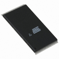
AT49BV8192A-90TC Atmel, AT49BV8192A-90TC Datasheet - Page 2

AT49BV8192A-90TC
Manufacturer Part Number
AT49BV8192A-90TC
Description
IC FLASH 8MBIT 90NS 48TSOP
Manufacturer
Atmel
Datasheet
1.AT49BV8192A-11CI.pdf
(20 pages)
Specifications of AT49BV8192A-90TC
Format - Memory
FLASH
Memory Type
FLASH
Memory Size
8M (1M x 8 or 512K x 16)
Speed
90ns
Interface
Parallel
Voltage - Supply
2.7 V ~ 3.6 V
Operating Temperature
0°C ~ 70°C
Package / Case
48-TSOP
Lead Free Status / RoHS Status
Contains lead / RoHS non-compliant
Other names
AT49BV8192A90TC
Note:
2
A
B
C
D
E
F
BYTE
GND
A13
A14
A15
A16
CBGA Top View (Ball Down)
1
“•” denotes a white dot on the package.
I/O14
I/O15
A11
A10
A12
I/O7
AT49BV/LV8192A(T)
2
AT49BV/LV008A(T)/8192A(T)
I/O13
I/O5
I/O6
WE
A8
A9
3
I/O11
I/O12
RST
VPP
I/O4
NC
4
VCC
A18
I/O2
I/O3
NC
NC
5
RESET
AT49BV/LV8192A(T) TSOP Top View
VPP
I/O10
A15
A14
A13
A12
A11
A10
A18
A17
WE
A17
I/O8
I/O9
NC
NC
NC
NC
NC
A9
A8
A7
A6
A5
A4
A3
A2
A1
A6
6
I/O0
I/O1
CE
1
2
3
4
5
6
7
8
9
10
11
12
13
14
15
16
17
18
19
20
21
22
23
24
A7
A5
A3
7
GND
OE
A4
A2
A1
A0
8
Type 1
The device contains a user-enabled “boot block” protection feature. Two versions of the
feature are available: the AT49BV/LV008A/8192A locates the boot block at lowest order
addresses (“bottom boot”); the AT49BV/LV008AT/8192AT locates it at highest order
addresses (“top boot”).
To allow for simple in-system reprogrammability, the AT49BV/LV008A(T)/8192A(T)
does not require high input voltages for programming. Reading data out of the device is
similar to reading from an EPROM; it has standard CE, OE and WE inputs to avoid bus
contention. Reprogramming the AT49BV/LV008A(T)/ 8192A(T) is performed by first
erasing a block of data and then by programming on a byte-by-byte or word-by-word
basis.
The device is erased by executing the Erase command sequence; the device internally
controls the erase operation. The memory is divided into four blocks for erase opera-
tions. There are two 4K word parameter block sections, the boot block, and the main
memory array block. The typical number of program and erase cycles is in excess of
10,000 cycles.
The optional 8K word boot block section includes a reprogramming lock out feature to
provide data integrity. This feature is enabled by a command sequence. Once the boot
block programming lockout feature is enabled, the data in the boot block cannot be
AT49BV/LV008A(T) Standard Pin Definition
48
47
46
45
44
43
42
41
40
39
38
37
36
35
34
33
32
31
30
29
28
27
26
25
A
B
C
D
E
F
A16
BYTE
GND
I/O15 / A-1
I/O7
I/O14
I/O6
I/O13
I/O5
I/O12
I/O4
VCC
I/O11
I/O3
I/O10
I/O2
I/O9
I/O1
I/O8
I/O0
OE
GND
CE
A0
CBGA Top View (Ball Down)
GND
A13
A14
A15
A16
NC
1
A11
A10
A12
I/O7
NC
A-1
2
I/O5
I/O6
WE
NC
A8
A9
3
VPP
RST
I/O4
NC
NC
NC
4
VCC
I/O2
I/O3
A18
NC
NC
5
A17
NC
NC
NC
NC
A6
6
I/O0
I/O1
CE
A7
A5
A3
7
RDY/BUSY
GND
OE
A4
A2
A1
A0
RESET
8
AT49BV/LV008A(T) TSOP Top View
VPP
A16
A15
A14
A13
A12
A11
A18
WE
A9
A8
A7
A6
A5
A4
A3
A2
A1
1
2
3
4
5
6
7
8
9
10
11
12
13
14
15
16
17
18
19
20
Type 1
A
B
C
D
E
F
GND
A14
A15
A16
A17
NC
AT49BV/LV008A(T) Alternate
CBGA Top View (Ball Down)
1
A12
A10
A13
A11
I/O7
NC
2
Pin Definition
WE
I/O5
I/O6
NC
A8
A9
3
40
39
38
37
36
35
34
33
32
31
30
29
28
27
26
25
24
23
22
21
VPP
RST
I/O4
NC
NC
NC
4
A17
GND
NC
A-1
A10
I/O7
I/O6
I/O5
I/O4
VCC
VCC
NC
I/O3
I/O2
I/O1
I/O0
OE
GND
CE
A0
VCC
1049K–FLASH–11/02
A19
I/O2
I/O3
NC
NC
5
A18
NC
NC
NC
NC
A6
6
I/O0
I/O1
CE
A7
A5
A3
7
GND
OE
A4
A2
A1
A0
8


