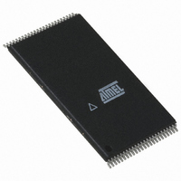
AT49BV8192AT-12TC Atmel, AT49BV8192AT-12TC Datasheet

AT49BV8192AT-12TC
Specifications of AT49BV8192AT-12TC
Available stocks
Related parts for AT49BV8192AT-12TC
AT49BV8192AT-12TC Summary of contents
Page 1
... I/O0 - I/O14 Data Inputs/Outputs I/O15 (Data Input/Output, Word Mode) I/O15 (A-1) A-1 (LSB Address Input, Byte Mode) BYTE Selects Byte or Word Mode NC No Connect 8-megabit ( 512K x 16) Flash Memory AT49BV008A AT49BV008AT AT49LV008A AT49LV008AT AT49BV8192A AT49BV8192AT AT49LV8192A AT49LV8192AT Rev. 1049K–FLASH–11/02 1 ...
Page 2
... The memory is divided into four blocks for erase opera- tions. There are two 4K word parameter block sections, the boot block, and the main memory array block. The typical number of program and erase cycles is in excess of 10,000 cycles. ...
Page 3
... DATA INPUTS/OUTPUTS I/O0 - I/O15 INPUT/OUTPUT BUFFERS PROGRAM DATA LATCHES Y-GATING 7FFFF 7FFFF BOOT BLOCK 8K WORDS 04000 7E000 03FFF 7DFFF PARAMETER BLOCK 1 4K WORDS 03000 7D000 02FFF 7CFFF PARAMETER BLOCK 2 4K WORDS 02000 7C000 01FFF 7BFFF MAIN MEMORY (496K WORDS) 00000 00000 3 ...
Page 4
... Boot Block Programming Lockout Override section). ERASURE: Before a byte or word can be reprogrammed, it must be erased. The erased state of memory bits is a logic “1”. The entire device can be erased by using the Chip Erase command or individual sectors can be erased by using the Sector Erase commands ...
Page 5
... TTL levels the boot block programming lockout feature is again active. PRODUCT IDENTIFICATION: The product identification mode identifies the device and manufacturer as Atmel. It may be accessed by hardware or software operation. The hardware operation mode can be used by an external programmer to identify the correct programming algorithm for the Atmel product. For details, see “ ...
Page 6
AT49BV/LV008A(T)/8192A(T) 6 TOGGLE BIT: In addition to Data Polling, the AT49BV/LV008A(T)/8192A(T) provides another method for determining the end of a program or erase cycle. During a program or erase operation, successive attempts to read data from the device will result ...
Page 7
... SA = 7FXXX for MAIN MEMORY ARRAY For the AT49BV/LV008AT/8192AT SA = 7FXXX for BOOT BLOCK SA = 7DXXX for PARAMETER BLOCK 7CXXX for PARAMETER BLOCK 7BXXX for MAIN MEMORY ARRAY Absolute Maximum Ratings* Temperature under Bias ................................ -55°C to +125°C Storage Temperature ..................................... -65°C to +150°C All Input Voltages (including NC Pins) with Respect to Ground ...
Page 8
... SA = FEXXX for MAIN MEMORY ARRAY For the AT49BV/LV008AT SA = FEXXX for BOOT BLOCK SA = FAXXX for PARAMETER BLOCK F8XXX for PARAMETER BLOCK F6XXX for MAIN MEMORY ARRAY Absolute Maximum Ratings* Temperature under Bias ................................ -55°C to +125°C Storage Temperature ..................................... -65°C to +150°C All Input Voltages (including NC Pins) with Respect to Ground ...
Page 9
DC and AC Operating Range Com. Operating Temperature (Case) Ind. V Power Supply CC Operating Modes Mode CE Read V IL (2) Program/Erase V IL Standby/Program V IH Inhibit Program Inhibit X Program Inhibit X Output Disable X Reset X ...
Page 10
AC Read Characteristics Symbol Parameter t Address to Output Delay ACC ( Output Delay CE ( Output Delay OE (3)( Output Float DF Output Hold from OE ...
Page 11
Input Test Waveforms and Measurement Level Output Test Load Pin Capacitance MHz ° C (1) Symbol Typ OUT Note: 1. This parameter is characterized and is not 100% tested. ...
Page 12
AC Word Load Characteristics Symbol Parameter Address, OE Setup Time AS OES t Address Hold Time AH t Chip Select Setup Time CS t Chip Select Hold Time CH t Write Pulse Width (WE or CE) WP ...
Page 13
Program Cycle Characteristics Symbol Parameter t Byte/Word Programming Time BP t Address Setup Time AS t Address Hold Time AH t Data Setup Time DS t Data Hold Time DH t Write Pulse Width WP t Write Pulse Width High ...
Page 14
Data Polling Characteristics Symbol Parameter t Data Hold Time Hold Time OEH ( Output Delay OE t Write Recovery Time WR Notes: 1. These parameters are characterized and not 100% tested. 2. See t ...
Page 15
Software Product Identification Entry LOAD DATA AA TO ADDRESS 5555 LOAD DATA 55 TO ADDRESS 2AAA LOAD DATA 90 TO ADDRESS 5555 ENTER PRODUCT IDENTIFICATION (2)(3)(5) MODE Software Product Identification Exit LOAD DATA (7) ADDRESS 5555 LOAD ...
Page 16
... AT49BV008A-90TI 40T Ordering Code Package AT49LV8192A-70TI 48T AT49LV8192AT-70TI 48T AT49BV8192A-90TI 48T AT49BV8192AT-90TI 48T AT49BV8192AT-90CI 48C1 Package Type Operation Range Industrial (-40° to 85°C) Industrial (-40° to 85°C) Operation Range Industrial (-40° to 85°C) Industrial (-40° to 85°C) 1049K–FLASH–11/02 ...
Page 17
Packaging Information 48C1 – CBGA Dimensions in Millimeters and (Inches). Controlling dimension: millimeters. 0.875 (0.034) REF 0.75 (0.0295) BSC NON-ACCUMULATIVE 2325 Orchard Parkway San Jose, CA 95131 R 1049K–FLASH–11/02 AT49BV/LV008A(T)/8192A(T) 7.10(0.280) 6.90(0.272 7.10(0.280) 6.90(0.272) TOP VIEW 5.25 (0.207) ...
Page 18
TSOP, Type 1 Pin 1 Identifier e E Notes: 1. This package conforms to JEDEC reference MO-142, Variation CD. 2. Dimensions D1 and E do not include mold protrusion. Allowable protrusion 0.15 mm per side ...
Page 19
TSOP Pin 1 Identifier e E Notes: 1. This package conforms to JEDEC reference MO-142, Variation DD. 2. Dimensions D1 and E do not include mold protrusion. Allowable protrusion 0.15 mm per side and on ...
Page 20
... No licenses to patents or other intellectual property of Atmel are granted by the Company in connection with the sale of Atmel products, expressly or by implication. Atmel’s products are not authorized for use as critical components in life support devices or systems. ...


