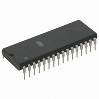
AT49F040-90PC Atmel, AT49F040-90PC Datasheet

AT49F040-90PC
Specifications of AT49F040-90PC
Related parts for AT49F040-90PC
AT49F040-90PC Summary of contents
Page 1
... Typical 10,000 Write Cycles Description The AT49F040 is a 5-volt-only in-system Flash Memory. Its 4 megabits of memory is organized as 524,288 words by 8 bits. Manufactured with Atmel’s advanced nonvola- tile CMOS technology, the device offers access times with power dissipation of just 275 mW over the commercial temperature range. When the device is dese- lected, the CMOS standby current is less than 100 µ ...
Page 2
... To allow for simple in-system reprogrammability, the AT49F040 does not require high input voltages for pro- gramming. Five-volt-only commands determine the read and programming operation of the device. Reading data out of the device is similar to reading from an EPROM. Reprogramming the AT49F040 is performed by erasing the entire 4 megabits of memory and then programming on a byte-by-byte basis ...
Page 3
... DATA polling may begin at any time during the program cycle. TOGGLE BIT: In addition to DATA polling the AT49F040 provides another method for determining the end of a pro- gram or erase cycle. During a program or erase operation, successive attempts to read data from the device will result in I/O6 toggling between one and zero ...
Page 4
... Temperature Under Bias................................ -55°C to +125°C Storage Temperature ..................................... -65°C to +150°C All Input Voltages (including NC Pins) with Respect to Ground ...................................-0.6V to +6.25V All Output Voltages with Respect to Ground .............................-0. Voltage on OE with Respect to Ground ...................................-0.6V to +13.5V AT49F040 4 1st Bus 2nd Bus 3rd Bus Cycle Cycle Cycle Addr ...
Page 5
... High Z ( A18 = Manufacturer Code ( A18 = Device Code A18 = V Manufacturer Code A18 = V Device Code IH IL Min Max 10 10 Com. 100 Ind. 300 3 50 0.8 2.0 0.45 2.4 4.2 AT49F040-12 0 ° ° C -40 ° ° ± 10% (4) (4) (4) (4) Units µA µA µA µ ...
Page 6
... AT49F040-70 Min Max Min after the address transition without impact on t ACC after the falling edge of CE without impact pF). L Output Test Load Max 6 12 AT49F040-90 AT49F040-12 Max Min Max Min Max 70 90 120 70 90 120 ACC after an address change CE ACC ...
Page 7
... Symbol Parameter t Address Hold Time AH t Chip Select Set-up Time CS t Chip Select Hold Time CH t Write Pulse Width ( Data Set-up Time Data, OE Hold Time DH OEH t Write Pulse Width High WPH AC Byte Load Waveforms WE Controlled CE Controlled AT49F040 Min Max Units ...
Page 8
... Data Setup Time DS t Data Hold Time DH t Write Pulse Width WP t Write Pulse Width High WPH t Erase Cycle Time EC Program Cycle Waveforms Chip Erase Cycle Waveforms Note: OE must be high only when WE and CE are both low. AT49F040 8 Min Typ Max Units µ ...
Page 9
... Toggle Bit Waveforms Notes: 1. Toggling either both OE and CE will operate toggle bit. The t input(s). 2. Beginning and ending state of I/O6 will vary. 3. Any address location may be used but the address should not vary. (1) (1) AT49F040 Min Typ Max Min Typ Max 10 10 ...
Page 10
... Manufacture Code is read for Device Code is read for The device does not remain in identification mode if powered down. 4. The device returns to standard operation mode. 5. Manufacturer Code: 1FH Device Code: 13H AT49F040 10 Boot Block Lockout Feature Enable Algorithm LOAD DATA F0 TO ANY ADDRESS ...
Page 11
... AT49F040-55JI 32J AT49F040-55PI 32P6 AT49F040-55TI 32T AT49F040-70JC 32J AT49F040-70PC 32P6 AT49F040-70TC 32T AT49F040-70JI 32J AT49F040-70PI 32P6 AT49F040-70TI 32T AT49F040-90JC 32J AT49F040-90PC 32P6 AT49F040-90TC 32T AT49F040-90JI 32J AT49F040-90PI 32P6 AT49F040-90TI 32T AT49F040-12JC 32J AT49F040-12PC 32P6 AT49F040-12TC 32T AT49F040-12JI 32J AT49F040-12PI 32P6 AT49F040-12TI ...
Page 12
... REF 0.70(.028) 0.50(.020) *Controlling dimension: millimeters AT49F040 12 32P6, 32-lead, 0.600" Wide, Plastic Dual Inline Package (PDIP) Dimensions in Inches and (Millimeters) .025(.635) X 30˚ - 45˚ .012(.305) .008(.203) .530(13.5) .490(12.4) ...
Page 13
... No licenses to patents or other intellectual property of Atmel are granted by the Company in connection with the sale of Atmel products, expressly or by implication. Atmel’s products are not authorized for use as critical components in life support devices or systems. ...


