AT25020A-10PU-2.7 Atmel, AT25020A-10PU-2.7 Datasheet

IC EEPROM 2KBIT 20MHZ 8DIP

AT25020A-10PU-2.7

Manufacturer Part Number
AT25020A-10PU-2.7
Description
IC EEPROM 2KBIT 20MHZ 8DIP
Manufacturer
Atmel

Specifications of AT25020A-10PU-2.7

Format - Memory
EEPROMs - Serial
Memory Type
EEPROM
Memory Size
2K (256 x 8)
Speed
10MHz, 20MHz
Interface
SPI, 3-Wire Serial
Voltage - Supply
2.7 V ~ 5.5 V
Operating Temperature
-40°C ~ 85°C
Package / Case
8-DIP (0.300", 7.62mm)
Capacitance, Input
6 pF
Capacitance, Output
8 pF
Current, Input, Leakage
-3 μA
Current, Operating
4.5 mA
Current, Output, Leakage
±3
Data Retention
100 yrs.
Density
2K
Organization
256×8
Package Type
PDIP
Temperature, Operating
-40 to +85 °C
Time, Access
40 ns
Time, Address Hold
100
Time, Address Setup
100
Time, Fall
2 μs
Time, Rise
2 μs
Voltage, Input, High
3.2 to 6 V
Voltage, Input, Low
0.81 to 1.65 V
Voltage, Output, High
1.9 V
Voltage, Output, Low
0.4 V
Voltage, Supply
2.7 to 5.5 V
Lead Free Status / RoHS Status
Lead free / RoHS Compliant

Available stocks

Company
Part Number
Manufacturer
Quantity
Price
Part Number:
AT25020A-10PU-2.7
Manufacturer:
TDK
Quantity:
2 122
Features
Description
The AT25010A/020A/040A provides 1024/2048/4096 bits of serial electrically eras-
able programmable read-only memory (EEPROM) organized as 128/256/512 words of
8 bits each. The device is optimized for use in many industrial and commercial appli-
c a t i o n s w h e r e l ow - p ow e r a n d l ow - vo l t a g e o p e ra t i o n a r e e s s e n t i a l . T h e
AT25010A/020A/040A is available in space saving 8-lead PDIP, 8-lead JEDEC SOIC,
8-lead Ultra Thin
The AT25010A/020A/040A is enabled through the Chip Select pin (CS) and accessed
via a three-wire interface consisting of Serial Data Input (SI), Serial Data Output (SO),
and Serial Clock (SCK). All programming cycles are completely self-timed, and no
separate erase cycle is required before write.
Block write protection is enabled by programming the status register with one of four
blocks of write protection. Separate Program Enable and Program disable instructions
are provided for additional data protection. Hardware data protection is provided via
the WP pin to protect against inadvertent write attempts. The HOLD pin may be used
to suspend any serial communication without resetting the serial sequence.
Table 1. Pin Configuration
Pin Name
CS
SCK
SI
SO
GND
VCC
WP
HOLD
Serial Peripheral Interface (SPI) Compatible
Supports SPI Modes 0 (0,0) and 3 (1,1)
Low-voltage and Standard-voltage Operation
20 MHz Clock Rate (5V)
8-byte Page Mode
Block Write Protection
Write Protect (WP) Pin and Write Disable Instructions for Both Hardware and Software
Data Protection
Self-timed Write Cycle (5 ms max)
High Reliability
Automotive Devices Available
8-lead JEDEC PDIP, 8-lead JEDEC SOIC, 8-lead Ultra Thin mini-MAP (MLP 2x3) and 8-
lead TSSOP Packages
Die Sales: Wafer Form, Waffle Pack, Bumped Wafers
– Data Sheet Describes Mode 0 Operation
– 2.7 (V
– 1.8 (V
– Protect 1/4, 1/2, or Entire Array
– Endurance: One Million Write Cycles
– Data Retention: 100 Years
CC
CC
Function
Chip Select
Serial Data Clock
Serial Data Input
Serial Data Output
Ground
Power Supply
Write Protect
Suspends Serial Input
= 2.7V to 5.5V)
= 1.8V to 5.5V)
mini-MAP (MLP 2x3)
, and 8-lead TSSOP packages.
8-lead Ultra Thin mini-MAP (MLP 2x3)
GND
HOLD
WP
VCC
SCK
CS
SO
SI
8
7
6
5
8-lead PDIP
Bottom view
1
2
3
4
8
7
6
5
1
2
3
4
CS
SO
WP
GND
VCC
HOLD
SCK
SI
G N D
G N D
W P
W P
S O
S O
C S
C S
8-lead TSSOP
1
2
3
4
1
2
3
4
8-lead SOIC
8
7
6
5
8
7
6
5
V C C
H O L
S C K
S I
V C C
H O L
S C K
S I
SPI Serial
EEPROM
1K (128x8)
2K (256x8)
4K (512x8)
AT25010A
AT25020A
AT25040A

Related parts for AT25020A-10PU-2.7

AT25020A-10PU-2.7 Summary of contents

Page 1

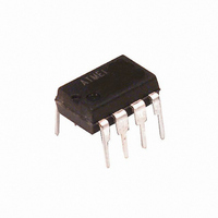
... Write Protect HOLD Suspends Serial Input , and 8-lead TSSOP packages. 8-lead SOIC 8-lead PDIP VCC HOLD SCK GND 8-lead Ultra Thin mini-MAP (MLP 2x3) 8-lead TSSOP VCC HOLD SCK GND Bottom view SPI Serial EEPROM 1K (128x8) 2K (256x8) 4K (512x8) AT25010A AT25020A AT25040A ...

Page 2

... This is a stress rating only and functional operation of the device at these or any other conditions beyond those indicated in the operational sections of this specification is not implied. Exposure to absolute maximum rating conditions for extended periods may affect device reliability. MEMORY ARRAY STATUS 128/256/512 X 8 REGISTER DATA REGISTER MODE ...

Page 3

Table 2. Pin Capacitance Applicable over recommended operating range from T Symbol Test Conditions C Output Capacitance (SO) OUT C Input Capacitance (CS, SCK, SI, WP, HOLD) IN Note: 1. This parameter is characterized and is not 100% tested. ...

Page 4

Table 4. AC Characteristics Applicable over recommended operating range from TTL Gate and 30 pF (unless otherwise noted) Symbol Parameter f SCK Clock Frequency SCK t Input Rise Time RI t Input Fall Time FI t ...

Page 5

Table 4. AC Characteristics (Continued) Applicable over recommended operating range from TTL Gate and 30 pF (unless otherwise noted) Symbol Parameter t Hold to Output Low Hold to Output High ...

Page 6

... AT25020A Ordering Information Ordering Code (2) AT25020A-10PU-2.7 (2) AT25020A-10PU-1.8 (2) AT25020AN-10SU-2.7 (2) AT25020AN-10SU-1.8 (2) AT25020A-10TU-2.7 (2) AT25020A-10TU-1.8 (2) AT25020AY1-10YU-1.8 (Not recommended for new designs) (3) AT25020AY6-10YH-1.8 (4) AT25020A-W1.8-11 Notes: 1. For 2.7V devices used in the 4.5 to 5.5V range, please refer to performance values in Table on page 3 and Table 4 on page 4. 2. “U” designates Green Package + RoHS compliant. ...

Page 7

Packaging Information 8P3 – PDIP Top View PLCS Side View Notes: 1. This drawing is for general information only; refer to JEDEC Drawing MS-001, Variation BA, for additional information. 2. Dimensions A and L are measured ...

Related keywords