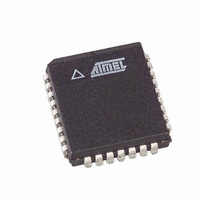
AT29C040A-12JU Atmel, AT29C040A-12JU Datasheet - Page 4

AT29C040A-12JU
Manufacturer Part Number
AT29C040A-12JU
Description
IC FLASH 4MBIT 120NS 32PLCC
Manufacturer
Atmel
Datasheet
1.AT29C040A-12PC.pdf
(17 pages)
Specifications of AT29C040A-12JU
Format - Memory
FLASH
Memory Type
FLASH
Memory Size
4M (512K x 8)
Speed
120ns
Interface
Parallel
Voltage - Supply
4.5 V ~ 5.5 V
Operating Temperature
-40°C ~ 85°C
Package / Case
32-PLCC
Lead Free Status / RoHS Status
Lead free / RoHS Compliant
Available stocks
Company
Part Number
Manufacturer
Quantity
Price
4.5
4.6
4.7
4.8
4
Hardware Data Protection
Product Identification
DATA Polling
Toggle Bit
AT29C040A
be performed. The software protection feature may be enabled or disabled by the user; when
shipped from Atmel, the software data protection feature is disabled. To enable the software
data protection, a series of three program commands to specific addresses with specific data
must be performed. After the software data protection is enabled the same three program com-
mands must begin each program cycle in order for the programs to occur. All software program
commands must obey the sector program timing specifications. The SDP feature protects all
sectors, not just a single sector. Once set, the software data protection feature remains active
unless its disable command is issued. Power transitions will not reset the software data protec-
tion feature, however the software feature will guard against inadvertent program cycles during
power transitions.
After setting SDP, any attempt to write to the device without the three-byte command sequence
will start the internal write timers. No data will be written to the device; however, for the duration
of t
After the software data protection’s 3-byte command code is given, a byte load is performed by
applying a low pulse on the WE or CE input with CE or WE low (respectively) and OE high. The
address is latched on the falling edge of CE or WE, whichever occurs last. The data is latched by
the first rising edge of CE or WE. The 256 bytes of data must be loaded into each sector by the
same procedure as outlined in the program section under device operation.
Hardware features protect against inadvertent programs to the AT29C040A in the following
ways: (a) V
power on delay – once V
out 5 ms (typical) before programming; (c) Program inhibit – holding any one of OE low, CE high
or WE high inhibits program cycles; and (d) Noise filter – pulses of less than 15 ns (typical) on
the WE or CE inputs will not initiate a program cycle.
The product identification mode identifies the device and manufacturer as Atmel. It may be
accessed by hardware or software operation. The hardware operation mode can be used by an
external programmer to identify the correct programming algorithm for the Atmel product. In
addition, users may wish to use the software product identification mode to identify the part
(i.e. using the device code), and have the system software use the appropriate sector size for
program operations. In this manner, the user can have a common board design for 256K to
4-megabit densities and, with each density’s sector size in a memory map, have the system soft-
ware apply the appropriate sector size.
For details, see Operating Modes (for hardware operation) or Software Product Identification.
The manufacturer and device code is the same for both modes.
The AT29C040A features DATA polling to indicate the end of a program cycle. During a pro-
gram cycle an attempted read of the last byte loaded will result in the complement of the loaded
data on I/O7. Once the program cycle has been completed, true data is valid on all outputs and
the next cycle may begin. DATA polling may begin at any time during the program cycle.
In addition to DATA polling the AT29C040A provides another method for determining the end of
a program or erase cycle. During a program or erase operation, successive attempts to read
WC
, a read operation will effectively be a polling operation.
CC
sense – if V
CC
CC
has reached the V
is below 3.8V (typical), the program function is inhibited; (b) V
CC
sense level, the device will automatically time
0333L–FLASH–9/08
CC


