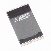
AT49BV002AN-70VU Atmel, AT49BV002AN-70VU Datasheet - Page 3

AT49BV002AN-70VU
Manufacturer Part Number
AT49BV002AN-70VU
Description
IC FLASH 2MBIT 70NS 32VSOP
Manufacturer
Atmel
Datasheet
1.AT49BV002A-70JI.pdf
(19 pages)
Specifications of AT49BV002AN-70VU
Format - Memory
FLASH
Memory Type
FLASH
Memory Size
2M (256K x 8)
Speed
70ns
Interface
Parallel
Voltage - Supply
2.7 V ~ 3.6 V
Operating Temperature
-40°C ~ 85°C
Package / Case
32-VSOP
Lead Free Status / RoHS Status
Lead free / RoHS Compliant
Available stocks
Company
Part Number
Manufacturer
Quantity
Price
Company:
Part Number:
AT49BV002AN-70VU
Manufacturer:
ATMEL
Quantity:
8 080
3. Block Diagram
4. Device Operation
4.1
4.2
3353G–FLASH–8/05
Read
Command Sequences
The AT49BV002A(N)(T) is accessed like an EPROM. When CE and OE are low and WE is high,
the data stored at the memory location determined by the address pins is asserted on the out-
puts. The outputs are put in the high impedance state whenever CE or OE is high. This dual-line
control gives designers flexibility in preventing bus contention.
When the device is first powered on it will be reset to the read or standby mode depending upon
the state of the control line inputs. In order to perform other device functions, a series of com-
mand sequences are entered into the device. The command sequences are shown in the
“Command Definition
the WE or CE input with CE or WE low (respectively) and OE high. The address is latched on the
falling edge of CE or WE (except for the sixth cycle of the Sector Erase command), whichever
occurs last. The data is latched by the first rising edge of CE or WE. Standard microprocessor
write timings are used. The address locations used in the command sequences are not affected
by entering the command sequences.
ADDRESS
INPUTS
RESET
GND
VCC
WE
OE
CE
Y DECODER
X DECODER
CONTROL
Table”. The command sequences are written by applying a low pulse on
LOGIC
DATA INPUTS/OUTPUTS
DATA LATCHES
AT49BV002A(N)
INPUT/OUTPUT
MAIN MEMORY
MAIN MEMORY
MAIN MEMORY
MAIN MEMORY
BOOT BLOCK
PARAMETER
PARAMETER
(64K BYTES)
(64K BYTES)
(64K BYTES)
(32K BYTES)
(16K BYTES)
(8K BYTES)
(8K BYTES)
PROGRAM
Y-GATING
I/O7 - I/O0
BUFFERS
BLOCK 4
BLOCK 3
BLOCK 2
BLOCK 1
BLOCK 2
BLOCK 1
8
AT49BV002A(N)(T)
3FFFF
30000
2FFFF
20000
1FFFF
10000
0FFFF
08000
07FFF
06000
05FFF
04000
03FFF
00000
DATA INPUTS/OUTPUTS
AT49BV002A(N)T
DATA LATCHES
INPUT/OUTPUT
MAIN MEMORY
MAIN MEMORY
MAIN MEMORY
MAIN MEMORY
BOOT BLOCK
PARAMETER
PARAMETER
(16K BYTES)
(32K BYTES)
(64K BYTES)
(64K BYTES)
(64K BYTES)
(8K BYTES)
(8K BYTES)
PROGRAM
Y-GATING
I/O7 - I/O0
BUFFERS
BLOCK 1
BLOCK 2
BLOCK 1
BLOCK 2
BLOCK 3
BLOCK 4
8
3FFFF
3C000
3BFFF
3A000
39FFF
38000
37FFF
30000
2FFFF
20000
1FFFF
10000
0FFFF
00000
3


