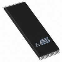
AT49F512-55TI Atmel, AT49F512-55TI Datasheet - Page 3

AT49F512-55TI
Manufacturer Part Number
AT49F512-55TI
Description
IC FLASH 512KBIT 55NS 32TSOP
Manufacturer
Atmel
Datasheet
1.AT49F512-55TI.pdf
(18 pages)
Specifications of AT49F512-55TI
Format - Memory
FLASH
Memory Type
FLASH
Memory Size
512K (64K x 8)
Speed
55ns
Interface
Parallel
Voltage - Supply
4.5 V ~ 5.5 V
Operating Temperature
-40°C ~ 85°C
Package / Case
32-TSOP
Lead Free Status / RoHS Status
Contains lead / RoHS non-compliant
Available stocks
Company
Part Number
Manufacturer
Quantity
Price
Part Number:
AT49F512-55TI
Manufacturer:
ATMEL/爱特梅尔
Quantity:
20 000
3. Block Diagram
4. Device Operation
4.1
4.2
4.3
1027H–FLASH–10/05
Read
Erasure
Byte Programming
The AT49F512 is accessed like an EPROM. When CE and OE are low and WE is high, the data
stored at the memory location determined by the address pins is asserted on the outputs. The
outputs are put in the high impedance state whenever CE or OE is high. This dual-line control
gives designers flexibility in preventing bus contention.
Before a byte can be reprogrammed, the 64K bytes memory array (or 56K bytes if the boot block
featured is used) must be erased. The erased state of the memory bits is a logical “1”. The entire
device can be erased at one time by using a 6-byte software code. The chip erase code consists
of 6-byte load commands to specific address locations with a specific data pattern (please refer
to the Chip Erase Cycle Waveforms).
After the chip erase has been initiated, the device will internally time the erase operation so that
no external clocks are required. The maximum time needed to erase the whole chip is t
boot block lockout feature has been enabled, the data in the boot sector will not be erased.
Once the memory array is erased, the device is programmed (to a logical “0”) on a byte-by-byte
basis. Please note that a data “0” cannot be programmed back to a “1”; only erase operations
can convert “0”s to “1”s. Programming is accomplished via the internal device command register
and is a 4 bus cycle operation (please refer to the Command Definitions table). The device will
automatically generate the required internal program pulses.
The program cycle has addresses latched on the falling edge of WE or CE, whichever occurs
last, and the data latched on the rising edge of WE or CE, whichever occurs first. Programming
is completed after the specified t
indicate the end of a program cycle.
BP
cycle time. The DATA polling feature may also be used to
AT49F512
FFFFH
2000H
1FFFH
0000H
EC
. If the
3


