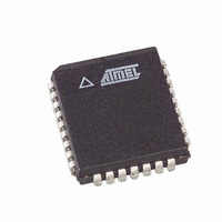
AT49LH00B4-33JX Atmel, AT49LH00B4-33JX Datasheet - Page 27

AT49LH00B4-33JX
Manufacturer Part Number
AT49LH00B4-33JX
Description
IC FLASH 4MBIT 33MHZ 32PLCC
Manufacturer
Atmel
Datasheet
1.AT49LH00B4-33JC.pdf
(41 pages)
Specifications of AT49LH00B4-33JX
Format - Memory
FLASH
Memory Type
FLASH
Memory Size
4M (512K x 8)
Speed
33MHz
Interface
Parallel
Voltage - Supply
3 V ~ 3.6 V
Operating Temperature
0°C ~ 85°C
Package / Case
32-PLCC
Lead Free Status / RoHS Status
Lead free / RoHS Compliant
Available stocks
Company
Part Number
Manufacturer
Quantity
Price
Part Number:
AT49LH00B4-33JX
Manufacturer:
AT
Quantity:
20 000
16. Command Definitions Table
Notes:
16.1
16.2
3379C–FLASH–3/05
Command
Read Array
Sector Erase
Uniform Sector
Erase
Byte Program
Read Status Register
Clear Status Register
Product ID Read
(1)(2)
1. The sector must not be hardware write protected or write-locked when attempting sector erase or program operations.
2. Sub-sectors are sectors 3, 2, 1, and 0; the main sectors are sectors 10 through 4. Refer to the Device Memory Map and
3. Either 40H or 10H is recognized by the device as the byte program command.
4. Following the Product ID Read command, read operations will access manufacturer and device ID information. Refer to
Read Array
Sector Erase
Attempts to issue a sector erase or byte program command to a hardware write protected or write-locked sector will fail.
Table 11-1
one time to allow uniform 64-Kbyte sectors to be erased. A Uniform Sector Erase command issued to any address in any
one of the sub-sectors will cause all the sub-sectors to be erased provided that all of the sub-sectors are not protected or
write-locked. The standard Sector Erase command can be used to erase both the sub-sectors and the main sectors, allow-
ing a single erase command to be used to erase any sector in the memory array.
Table 16-2
(1)(2)
(1)(3)
(4)
for sector sizes and address ranges. The Uniform Sector Erase command can be used to erase all sub-sectors at
for Product ID addresses and data.
Command
Cycles
1+
Upon initial device power-up and after exit from reset, the device defaults to the read array
mode. This operation is also initiated by writing the Read Array command. The device remains
enabled for reads until another command is written to the device.
Once the internal write state machine (WSM) has started a sector erase or program operation,
the device will not recognize the Read Array command until the operation is completed.
Before a byte can be programmed into a sector, the sector must first be erased. The memory
array is organized into multiple sectors that can be individually erased using two different sector
erase commands, Sector Erase and Uniform Sector Erase. The Uniform Sector Erase command
can be used to erase the main sectors, and it can also be used to erase all of the sub-sectors to
allow the memory array to be erased in uniform 64-Kbyte regions. The Sector Erase command is
used to erase the individual sub-sectors to provide a more efficient and finer erase granularity. In
addition, the Sector Erase command can be used to erase the main sectors as well to allow a
single erase command to be used to erase any sector in the memory array. Both sector erase
commands require two command cycles to initiate the internally self-timed erase operation.
After issuing a sector erase command, the device’s Status Register may be checked to deter-
mine the status of the WSM and the erase operation. If the device detects a sector erase error,
the Status Register should be cleared before the system software attempts any corrective
2
2
2
2
1
2
Type
Write
Write
Write
Write
Write
Write
Write
1st Command Cycle
Address
Any Address
Any Address in
the Sector
Any Address in
the Sector
The Address to
be Programmed
Any Address
Any Address
Any Address
40H or 10H
Data
FFH
21H
20H
70H
50H
90H
Read
Write
Write
Read
Read
Type
Write
2nd Command Cycle
Address
Any Address
Any Address in
the Sector
Any Address in
the Sector
The Address to
be Programmed
Any Address
ID Address
AT49LH00B4
Data OUT
Register
Data IN
ID Data
Status
Data
D0H
D0H
Data
27


