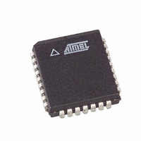
AT49LW080-33JC SL383 Atmel, AT49LW080-33JC SL383 Datasheet - Page 18

AT49LW080-33JC SL383
Manufacturer Part Number
AT49LW080-33JC SL383
Description
IC FLASH 8MBIT 33MHZ 32PLCC
Manufacturer
Atmel
Datasheet
1.AT49LW080-33JC.pdf
(34 pages)
Specifications of AT49LW080-33JC SL383
Format - Memory
FLASH
Memory Type
FLASH
Memory Size
8M (1M x 8)
Speed
33MHz
Interface
Parallel
Voltage - Supply
3 V ~ 3.6 V
Operating Temperature
0°C ~ 85°C
Package / Case
32-PLCC
Lead Free Status / RoHS Status
Contains lead / RoHS non-compliant
7.3
7.4
7.5
18
Sector Erase
Byte Programming
Erase Suspend
AT49LW080
Before a byte can be programmed, it must be erased. The erased state of the memory bits is a
logical “1”. Since the AT49LW080 does not offer a complete chip erase, the device is organized
into multiple sectors that can be individually erased. The Sector Erase command is a two-bus
cycle operation.
Successful sector erase requires that the corresponding sector’s Write Lock bit be cleared and
the corresponding write-protect pin (TBL or WP) be inactive. If sector erase is attempted when
the sector is locked, the sector erase will fail, with the reason for failure in the status register.
Successful sector erase only occurs when V
attempted at V
The device is programmed on a byte-by-byte basis. Programming is accomplished via the inter-
nal device command register and is a two-bus cycle operation. The programming address and
data are latched in the second bus cycle. The device will automatically generate the required
internal programming pulses. Please note that a “0” cannot be programmed back to a “1”; only
an erase operation can convert “0”s to “1”s.
After the program command is written, the device automatically outputs the status register data
when read. When programming is complete, the status register may be checked. If a program
error is detected, the status register should be cleared before corrective action is taken by the
software. The internal WSM verification Error Checking only detects “1”s that do not successfully
program to “0”s.
Reliable programming only occurs when V
attempted at V
A successful program operation also requires that the corresponding sector’s Write Lock bit be
cleared, and the corresponding write-protect pin (TBL or WP) be inactive. If a program operation
is attempted when the sector is locked, the operation will fail.
The Erase Suspend command allows sector-erase interruption to read or program data in
another sector of memory. Once the sector erase process starts, writing the sector erase sus-
pend command requests that the WSM suspend the sector erase sequence at a predetermined
point in the algorithm. The device outputs status register data when read after the sector erase
suspend command is written. Polling the status register can help determine when the sector
erase operation was suspended. After a successful suspend, a Read Array command can be
written to read data from a sector other than the suspended sector. A program command
sequence may also be issued during erase suspend to program data in sectors other than the
sector currently in the erase suspend mode.
The other valid commands while sector erase is suspended include Read Status Register and
Sector Erase Resume. After a Sector Erase Resume command is written, the WSM will continue
the sector erase process. V
erase) while sector erase is suspended. RST or INIT must also remain at V
not resume until program operations initiated during sector erase suspend have completed.
PP
PP
≠ V
≠ V
PPH1
PPH1
or V
or V
PP
PPH2
PPH2
must remain at V
erratic results may occur.
erratic results may occur.
PP
PPH1/2
PP
= V
= V
PPH1
(the same V
PPH1
or V
or V
PPH2
PPH2
PP
. If the program operation is
level initially used for sector
. If the erase operation is
IH
. Sector erase can-
1966G–FLASH–3/05


