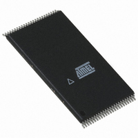
AT49BV642D-70TU Atmel, AT49BV642D-70TU Datasheet - Page 6

AT49BV642D-70TU
Manufacturer Part Number
AT49BV642D-70TU
Description
IC FLASH 64MBIT 70NS 48TSOP
Manufacturer
Atmel
Datasheet
1.AT49BV642D-70TU.pdf
(29 pages)
Specifications of AT49BV642D-70TU
Format - Memory
FLASH
Memory Type
FLASH
Memory Size
64M (4M x 16)
Speed
70ns
Interface
Parallel
Voltage - Supply
2.7 V ~ 3.6 V
Operating Temperature
-40°C ~ 85°C
Package / Case
48-TSOP
Lead Free Status / RoHS Status
Lead free / RoHS Compliant
Available stocks
Company
Part Number
Manufacturer
Quantity
Price
Company:
Part Number:
AT49BV642D-70TU
Manufacturer:
Atmel
Quantity:
135
3.8
3.9
3.10
6
Erase Suspend/Erase Resume
Program Suspend/Program Resume
128-Bit Protection Register
AT49BV642D(T)
The Erase Suspend command allows the system to interrupt a sector erase operation and then
program or read data from a different sector within the memory. After the Erase Suspend com-
mand is given, the device requires a maximum time of 15 µs to suspend the erase operation.
After the erase operation has been suspended, the system can then read data or program data
to any other sector within the device. An address is not required during the Erase Suspend com-
mand. During a sector erase suspend, another sector cannot be erased. To resume the sector
erase operation, the system must write the Erase Resume command. The Erase Resume com-
mand is a one-bus cycle command. The device also supports an erase suspend during a
complete chip erase. While the chip erase is suspended, the user can read from any sector
within the memory that is protected. The command sequence for a chip erase suspend and a
sector erase suspend are the same.
The Program Suspend command allows the system to interrupt a programming operation and
then read data from a different word within the memory. After the Program Suspend command is
given, the device requires a maximum of 10 µs to suspend the programming operation. After the
programming operation has been suspended, the system can then read from any other word
within the device. An address is not required during the program suspend operation. To resume
the programming operation, the system must write the Program Resume command. The
program suspend and resume are one-bus cycle commands. The command sequence for the
erase suspend and program suspend are the same, and the command sequence for the erase
resume and program resume are the same.
The AT49BV642D(T) contains a 128-bit register that can be used for security purposes in sys-
tem design. The protection register is divided into two 64-bit blocks. The two blocks are
designated as block A and block B. The data in block A is non-changeable and is programmed
at the factory with a unique number. The data in block B is programmed by the user and can be
locked out such that data in the block cannot be reprogrammed. To program block B in the pro-
tection register, the four-bus cycle Program Protection Register command must be used as
shown in the
lock protection register command must be used as shown in the Command Definition table. Data
bit D1 must be zero during the fourth bus cycle. All other data bits during the fourth bus cycle are
don’t cares. To determine whether block B is locked out, the status of Block B Protection com-
mand is given. If data bit D1 is zero, block B is locked. If data bit D1 is one, block B can be
reprogrammed. Please see the
address locations in the protection register. To read the protection register, the Product ID Entry
command is given followed by a normal read operation from an address within the protection
register. After determining whether block B is protected or not or reading the protection register,
the Product ID Exit command must be given prior to performing any other operation.
“Command Definition Table” on page
“Protection Register Addressing Table” on page 12
11. To lock out block B, the four-bus cycle
3631A–FLASH–04/06
for the


